
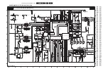
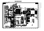


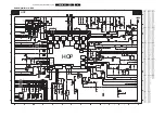
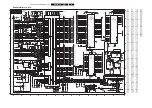
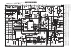

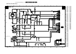


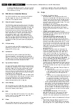

Circuit Diagrams and PWB Layouts
69
EM5.2E AA
7.
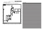
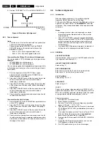
CRT Panel
Blue
Green
Red
V
200V
83V
3V
B
C
D
E
F
G
H
0031 F7
1237-A G13
1237-B G9
1237-C G11
1237-D E9
1237-E G12
1237-F F9
1237-G F9
1237-H H9
1237-I E9
1298-A G12
1298-B G12
1298-C G11
1298-D E9
1298-E G12
1298-F F9
1298-G G9
1298-H G9
1298-I E9
1298-J G9
1298-K H9
1424 H1
134V
B
1424
1
2
3
4
5
6
3V
7
8
9
10
11
12
13
14
1
2
3
4
5
6
7
8
9
10
11
12
13
14
A
B
C
D
E
F
G
H
A
R-CRT
220V
G
*
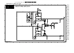
RGB AMPLIFIER
R
136V
AQUADAC
FOCUSA
1434 H13
1435 D9
1483 B13
1940 D2
2300 A8
2301 A5
2302 A5
2304 A8
2306 C6
2307 B8
2309 C8
2313 F4
2315 B5
2316 F5
2317 H13
2318 H11
2319 G7
2320 F6
2321 E5
2322 E5
2323 F5
2324 H13
2325 A7
0V7
3V
LINE DEFLECTION
*
SIM CONN.
FROM
B
LINE DEFLECTION
136V
FROM
2330 B8
2332 C2
2333 C2
2334 D2
2336 H7
2403 H6
2404 H6
2405 H5
2406 H6
2407 G6
2408 H7
2409 C7
2410 B3
2411 B5
2412 C4
2420 A7
2421 C11
2422 C9
2423 B9
2424 A10
2425 G2
2426 C4
FROM
VG
1
136V
136V
0V
LOT
8V1
G
CUT OFF
SCAVEM
3V
0V
Y-SCAVEM ln
FOCUSB
220V
EHT
3300 A5
3301 A8
3302 A7
3303 A6
3304 A8
3306 B7
3307 B6
3308 B8
3310 B13
3311 C6
3312 C6
3316 C8
3318 C8
3319 C8
3323 B7
GND LS2
0V
41V
2V5
VG
2
R
0V
0V
CRT PANEL
5V7
SCAVEM
0V
1V8
0V
0V
3324 B8
3325 B5
3329 B7
3334 H10
3335 E5
3336 F5
3337 E5
3338 F8
3339 E8
3340 E8
3341 F4
3342 D4
3345 G7
3347 H12
3349 H11
3350 E7
3V2
1V8
3V
0V5
1099
+8V
2K7
0V
TO
2V5
3351 E7
3352 F7
3354 F6
3355 A9
3356 B12
3357 C9
3358 C2
3359 C2
3360 D2
3370 H11
3401 G4
3402 G7
3403 H3
3404 G3
3405 C7
3410 B3
3411 B3
3412 A4
3413 C4
3414 B4
3416 A7
3417 G2
0V
TO
COIL
41V
1940
6V
3418 B5
3419 A8
3420 A10
3421 A10
3422 A10
3423 B10
3424 B10
3425 B10
3426 C10
3427 D10
3428 A6
3429 C4
3999 F2
5300 B11
5302 A11
5303 B11
5400 H4
6300 B7
6301 B7
6305 E7
6306 E7
6307 F7
6310 F6
6401 H5
7300 A6
7301 A7
EHT-INFO
G-CRT
5V6
TUNER and
7302 A10
7303 C10
7304 C7
7307 E5
7308 B4
7309 A10
7310 B10
9310 A12
9311 B12
9317 B11
9318 B11
9320 F2
9321 F2
9400 G7
9401 H5
9402 A11
9403 C11
9404 A8
9405 E2
9406 G6
9407 G4
9408 G4
9409 C4
9410 B4
9411 G3
9412 G9
9413 G9
9414 G1
FROM LOT
0V
311V
9416 H9
F004 F4
F013 H13
F017 F9
F018 E9
F019 E9
F020 G9
F021 H13
F128 G9
F130 H9
F148 E4
F149 E4
F151 E3
F155 F3
F156 F2
F157 F1
F158 H3
I100 A5
I101 A5
I102 A6
I103 A8
I104 A11
I105 D9
I106 A6
I108 B7
I109 B7
I110 A6
I111 B6
I112 B3
3V
B-CRT
EHT-INFO
RES
84V
2V5
0V7
2K7
I113 B3
I114 B3
I115 B6
I116 B4
I117 B5
I118 B4
I119 G11
I120 B8
I121 C8
I122 B4
I125 D5
I126 E5
I127 E6
I129 E7
I130 E5
I131 E6
I133 E7
I134 F5
I135 F6
I136 G11
I137 F7
I138 F4
0V
RES
I139 A7
I140 F6
I141 H13
I142 H12
I144 B8
I146 B11
I147 D3
I148 A10
I151 B10
I152 D3
I153 B4
I155 C10
I156 G4
I157 D3
I162 E2
I163 H8
I164 B12
I165 B12
I166 A10
I167 C9
I168 B5
I169 A9
I170 A8
I171 C9
I172 C9
I173 A5
I174 A6
Filament Pulses
I176 A7
I177 B7
I178 B7
I179 B7
I180 B8
I182 B7
I184 G2
I185 G2
I186 G3
I187 G3
I188 G4
I189 H3
I191 B11
I192 G5
I193 G6
I194 G6
I196 A7
I197 A7
I198 B7
I199 C7
470n
2426
CRT
F151
22n
2318
I129
GND_LS1
0031
PTP-EMGS
3n3
2425
BAS321
6307
GND_RGB
I100
I193
18p
2334
1K
3310
33R
3345
2
I115
FG1
1298-A
1
FG2
1298-B
3404
3R3
3312
2K2
F5
GND_RGB
2307
GND1
1298-J
12
I177
22n
BF824
7304
I189
I126
GND_RGB
2300
22u
I164
3419
I198
470R
3342
F156
3303
1K8
I169
2315
220p
I130
BCP56
7303
I142
VO2
8
VO3
7
2403
100u
RES
7307
TDA6108JF
4
GND
IOM
5
VDD
6
VI1
1
VI2
2
VI3
3
VO1
9
10n
2319
I121
GND_RGB
9402
GND_RGB
100K
3428
GNDB
1298-K
13
330R
3429
1
9406
I165
I137
1435
9411
1K
3340
3338
1K
I146
I176
3337
F155
3403
3R3
GND_LS1
18p
2332
I192
I172
7
33K
3426
GND_RGB
F4
G2
1298-E
3319
820R
I162
3307
10R
I167
10R
3357
RES
I147
10
11
2
3
4
5
6
7
8
9
F10
9408
10
1940
1
I116
9401
H1
1237-G
470p
2405 RES
GND_RGB
F018
I103
3300
10R
F020
3336
10K
3359
RES
22n
2304
RES
2323
68p
150R
3402
10n
2406
H1
1298-H
10
200V
9
F148
H2
1298-G
3
4
5
6
7
3411
100K
GND_RGB
1424
1
2
330R
3413
9311
6300
MCL4148
1K5
3422
GND_RGB
I131
I105
I144
33K
3423
33K
3421
9412
3318
+8V
470n
2410
1237-D
7
I122
F013
CG
1
10
3
5
6
I125
4R7
3323
S13974
5300
1298-F
8
3302
1K5
GND_SSB
CB
1298-I
11
CR
3412
15R
9317
I187
GND_RGB
1K2
3999
100K
3410
3355
10R
I110
9320
56R
3311
9416
RES
2404
100u
RES
I155
2324
F6
1434
PCB-TAB4.8x0.5
1
2
2421
GND_RGB
I118
10K
3360
I117
2325
100n
GND_RGB
3354
2K2
GND_LS1
I174
I166
100K
3316
I120
I152
I106
6401
BYV29X-500
RES
GND_RGB
3356
1K
GND_RGB
2320
100n
5303
+8V
22n
2309
CR
1237-F
9
GND_RGB
5302
9407
4R7
3329
100R
3401
F3
BCP53
7302
I194
9404
12
I156
I170
CB
1237-I
I196
10K
3358
F019
10R
3414
I141
3351
470R
GND_RGB
6p8
2302
BFS20
7300
F021
3334
1K
I135
I182
3335
I148
820R
3304
10n
2407
RES
F11
I138
9410
RES
GND_SSB
3n3
2408
3349
1K
3301
GND_LS1
I102
10n
2336
2409
470n
2317
F017
I104
9310
I178
F8
I168
7310
BCP56
F7
6301
MCL4148
G1
1237-C
6
F004
BAS321
6305
GND_RGB
GND_RGB
22n
2422
I127
I188
F15
3308
100K
I136
2301
220u
9413
9318
9321
3306
I199
5
H2
1237-H
11
I185
GND
1237-B
I134
I191
7308
BFS20
BFS20
7301
I186
I184
I113
I114
GND_RGB
I112
I180
1
3352
470R
I119
2424
SG1
1237-A
I197
F149
3341
150R
RES
GND_LS1
I111
39R
3416
9405
3325
F2
I151
I153
F130
1483
1
2
3
I157
F158
1K
3339
+8V
1K5
3425
I140
9409
GND_LS1
3405
39R
+8V
RES
200V
MCL4148
6310
F9
I179
33p
2412
3427
I171
2411
100n
100n
2306
3370
2322593
F13
GND_RGB
GND_RGB
9414
I173
2330
6
10R
3417
F128
SC3
CG
1298-D
10R
3418
GND_RGB
2316
100n
F14
F1
GND_SSB
1K5
3347
I109
F12
I133
5400
22u
9400
RES
+8V
I108
470n
2420
I101
8
3420
RES
I139
G2
1237-E
18p
2333
2313
10u
+8V
F157
3424
33K
GND_RGB
BCP53
7309
RES
I163
9403
68p
2322
3350
470R
G1
1298-C
5
6306
BAS321
2321
68p RES
3324
2423
22n
HFB_X-RAY-PROT
X-RAY-PROT_HFB
E_14600_024.eps
101204
3104 313 6567.4
F
F
CRT ECO PANEL


