Technical Specifications, Connections, and Chassis Overview
EN 3
1.
1.3
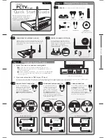
Chassis Overview
Figure 1-3 PWB location
MAINS SWITCH (PV2 & FL9)
LARGE SIGNAL PANEL
CRT/SCAVEM PANEL
F
J
TOP CONTROL PANEL
(styling FL9)
P
P
A
DC-SHIFT
(optional)
G
VDAF + 2nd ORDERS PANEL
I
SMALL SIGNAL BOARD
P
B
CL 36532061_042.eps
020903
SIDE I/O PANEL
O
D
N
JACK HIGH
DEFINITION INTERFACE
TOP CONTROL PANEL
(styling PV2)
P
P
or
&
Summary of Contents for EM1.1A
Page 35: ...Circuit Diagrams and PWB Layouts 35 EM1 1A AA 7 Layout LSP Top Side ...
Page 37: ...Circuit Diagrams and PWB Layouts 37 EM1 1A AA 7 Layout LSP Overview Bottom Side ...
Page 38: ...38 EM1 1A AA 7 Circuit Diagrams and PWB Layouts Layout LSP Part 1 Bottom Side ...
Page 39: ...Circuit Diagrams and PWB Layouts 39 EM1 1A AA 7 Layout LSP Part 2 Bottom Side ...
Page 40: ...40 EM1 1A AA 7 Circuit Diagrams and PWB Layouts Layout LSP Part 3 Bottom Side ...
Page 41: ...Circuit Diagrams and PWB Layouts 41 EM1 1A AA 7 Layout LSP Part 4 Bottom Side ...
Page 116: ...116 EM1 1A AA 7 Circuit Diagrams and PWB Layouts Personal Notes E_06532_013 eps 131004 ...