Circuit Descriptions, Abbreviation List, and IC Data Sheets
9.
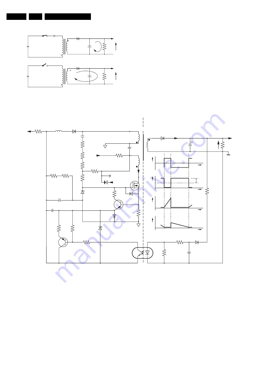
Figure 9-3 Flyback principle
After closing switch 'S,' the current ID will increase linearly in
time. The magnetic energy in the primary coil is directly
proportional with the self-inductance of the coil and current ID
(thus with the time the switch is closed).
The voltage polarity at the secondary winding is negative (due
to different winding direction), meaning that diode D will block.
Capacitor C will discharge via R
L
, and U
OUT
will decrease.
Opening switch 'S' will generate a counter-e.m.f. in the primary
winding, trying to maintain current I
D
. Through this the polarity
of the secondary voltage will inverse. The magnetic energy
stored in the coil will now be transformed to the secondary side.
Diode D will now conduct, capacitor C will be charged, and
U
OUT
will increase.
Implementation
Figure 9-4 Standby supply circuitry
To apply this on the EM1.1A(diagram A2): replace switch 'S' by
FET TS7102, coil L by L5100, diode D by D6111, and C by
C2104.
•
Time interval t0-t1: After switching 'on' the TV-set, the
gate of MOSFET TS7102 will be high (max. 15 V due to
zener diode D6105). This will drive the FET into saturation
(UDS = 0 V). The DC-voltage UMAINS will be transposed
across the primary winding of L5100 (3, 5), resulting in a
linear increasing current through this coil. The voltage
across the co-coupled coil (1, 2) is also positive and will
keep the FET in conductivity via C2101, R3103/3105/3102
and R3117 for some time. The self-induction of the coil and
the magnitude of the supply voltage (+375 V) determine the
slope of the primary current. The maximum current is
determined by the time the FET stays in conductance (t0-
t1). This time is directly determined by the voltage across
R3108//R3118 (0.7
Ω
). This voltage is a measure of the
current, and if it exceeds 1.4 V, TS7101 will be driven into
conductivity and consequently connects the gate of
TS7102 to earth. The FET will block. The current is: 1.4 V
/ 0.7
Ω
= 2 A. The voltage across the secondary winding (8,
9) will be negative, diodes D6111 and D6107 will block.
•
Time interval t1-t2: The sudden current interruption in the
primary coil will induce a counter-e.m.f. that tries to
maintain the current. The voltage on the drain of the FET
will increase. The secondary voltage (8, 10) will become
positive and will charge C2104 via D6111. All energy that
was stored in L5100 during t0-t1 will be transferred into the
load. Due to the transformer principle, a voltage will now
be induced in the primary winding (3, 5) and the co-coupled
winding (1, 2). This voltage will be N* U
SEC
(N= winding
ratio). The voltage across the co-coupled coil will be
negative, keeping the FET blocked.
•
Time t2: At t2, the current through the secondary coil will
be reduced to zero, as C2104 is no longer charged.
Consequently, the voltages will decay and will change
polarity. The gate of the FET will be again made positive, is
driven into conductivity, and the cycle starts again.
96532156_020.eps
210100
+
-
-
+
-
-
+
+
RL
D
Id
Uout
C
+
C
+
375V
S
RL
D
Uout
375V
S
Isec
CL 26532041_062.eps
110602
3103
1K
3105
1K
3113
22R
3124
6122
68R
3V9
RL
7101
6105
15V
3102
1K
3117
47R
3126
10K
3125
15R
7100
3104
47R
3101
STARTUP
V-START
10M
3127
5K6
3120
10R
3106
3107
1K
1K
2101
2n2
5102
-13V
6111
6103
U
MAINS
U
OUT
2104
2m2
D
S
G
6106
15V
3114
220R
2109 +
2149
6108
3108
//3118
+5V2
8
10
HOT
COLD
GND-STB
GND-STB
2
1
5
3
2114
7102
6105
15V
10n
2102
10
µ
+
U
A
UA
U
D
UD
UMAIN
I
SEC
I
PRIM
IPRIM
ISEC
7103/7104
t
t
t
t
N.Usec
ON
OFF
t0
t1
t2
5100/5101
3110
2R2
+375V
2111
Summary of Contents for Chassis EM1.1A AA
Page 51: ...Circuit Diagrams and PWB Layouts 51 EM1 1A AA 7 Layout LSP Top Side ...
Page 53: ...Circuit Diagrams and PWB Layouts 53 EM1 1A AA 7 Layout LSP Overview Bottom Side ...
Page 54: ...54 EM1 1A AA 7 Circuit Diagrams and PWB Layouts Layout LSP Part 1 Bottom Side ...
Page 55: ...Circuit Diagrams and PWB Layouts 55 EM1 1A AA 7 Layout LSP Part 2 Bottom Side ...
Page 56: ...56 EM1 1A AA 7 Circuit Diagrams and PWB Layouts Layout LSP Part 3 Bottom Side ...
Page 57: ...Circuit Diagrams and PWB Layouts 57 EM1 1A AA 7 Layout LSP Part 4 Bottom Side ...
Page 126: ...Revision List EN 126 EM1 1A AA 11 11 Revision List First release ...


