EN
26
Enable the PIN
1
Open the
P
a
re
ntal cont
ro
l
men
u.
2
Se
lect
Use PIN
and pr
ess
OK
.
>
T
he available options sho
w
.
3
Choose t
h
e pr
e
fer
re
d opt
ion and pr
ess
OK
.
/i
Change the rating le
ve
l
1
Open the
P
a
re
ntal cont
ro
l
men
u.
2
Se
lect
Rating le
v
e
l
and pr
ess
OK
.
>
T
he available options sho
w
.
3
Choose t
h
e pr
e
fer
re
d opt
ion and pr
ess
OK
.
Change the PIN
1
Open the
P
a
re
ntal cont
ro
l
men
u.
2
Se
lect
Ne
w
PIN
and pr
ess
OK
.
3
Fo
llo
w the on-scr
ee
n instruct
ions.
On
Of
f
U
se PIN
New PIN
R
ating lev
el
Pa
rental control
Option
Desc
rip
tion
On
The PI
N is
enable
d.
Off
The PI
N is
disabled
.
8 (A
dults)
7
6
5
4
3
U
se PIN
New PIN
R
ating lev
el
Pa
rental control
For example, when you set the rating leve
l to 6, discs with rating levels 7 and 8
cannot be played.
U
se PIN
Ent
er new PIN
New PIN
R
ating lev
el
Pa
rental control
EN
27
Enjo
y
T
u
rn the pr
oduct on
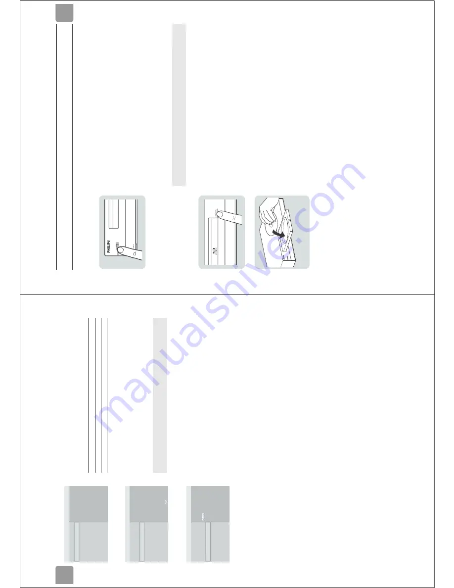
1
Set the TV to the cor
rect external input.
2
On the fr
ont
of
the pr
od
uct
, pr
e
ss the
ST
ANDBY/ON
button.
>T
h
e
ST
ANDBY/ON
ligh
t comes on as blue
.
Load a disc
1
T
u
rn the pr
oduct on.
2
Pr
ess the
OPE
N/
CLOS
E
button.
>
T
he disc tr
ay open
s.
3
Place the disc in th
e
disc tra
y.
4
Pr
ess the
OPE
N/
CLOS
E
button again.
>
T
he disc tr
ay c
loses
.
Be
fore you load a disc into the Blu-ray Disc
playe
r, make sure that the disc type is
supported. Refer to ’Playa
ble discs’ on page 37.
Summary of Contents for BDP9000
Page 8: ...EN 8 4 BDP9000 Technical Reference 4 1 2 Wiring Diagram Figure 4 1 2 ...
Page 12: ...EN 12 4 BDP9000 Technical Reference 4 5 Video Driver SM5302 block diagram VIC3 Figure 4 5 1 ...
Page 36: ...EN 36 9 BDP9000 Circuit Diagrams and PWB Layouts 9 2 SMPS SMPS PCB Figure 9 2 1 ...
Page 40: ...EN 40 9 BDP9000 Circuit Diagrams and PWB Layouts 9 6 S5L3700 DDR Memory Main PCB Figure 9 6 1 ...
Page 42: ...EN 42 9 BDP9000 Circuit Diagrams and PWB Layouts 9 8 S5L3700 Power GND Main PCB Figure 9 8 1 ...
Page 43: ...Circuit Diagrams and PWB Layouts BDP9000 9 EN 43 9 9 DDR Termination C Main PCB Figure 9 9 1 ...
Page 45: ...Circuit Diagrams and PWB Layouts BDP9000 9 EN 45 9 11 ATA ATAPI Main PCB Figure 9 11 1 ...
Page 46: ...EN 46 9 BDP9000 Circuit Diagrams and PWB Layouts 9 12 S5L3700 Video In Main PCB Figure 9 12 1 ...
Page 50: ...EN 50 9 BDP9000 Circuit Diagrams and PWB Layouts 9 16 DMN8602 DDR Main PCB Figure 9 16 1 ...
Page 55: ...Circuit Diagrams and PWB Layouts BDP9000 9 EN 55 9 21 Power Main PCB Figure 9 21 1 ...
Page 59: ...Circuit Diagrams and PWB Layouts BDP9000 9 EN 59 9 25 Front Front PCB Figure 9 25 1 ...
Page 60: ...EN 60 9 BDP9000 Circuit Diagrams and PWB Layouts 9 26 MEMORY CAED MEMORY PCB Figure 9 26 1 ...
Page 61: ...Circuit Diagrams and PWB Layouts BDP9000 9 EN 61 9 27 POWER SUB PCB Figure 9 27 1 ...
Page 66: ...EN 66 9 BDP9000 Circuit Diagrams and PWB Layouts 9 32 Front PCB component side Figure 9 32 1 ...
Page 67: ...Circuit Diagrams and PWB Layouts BDP9000 9 EN 67 9 33 Front PCB conductor side Figure 9 33 1 ...
Page 68: ...EN 68 9 BDP9000 Circuit Diagrams and PWB Layouts 9 34 Memory Key PCB Figure 9 34 1 ...
Page 69: ...Circuit Diagrams and PWB Layouts BDP9000 9 EN 69 9 35 Front Key PCB Figure 9 35 1 ...
Page 73: ...Directions for Use BDP9000 11 EN 73 11 Directions for Use ...


