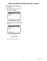
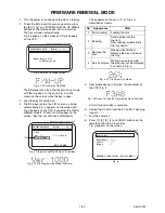
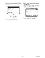
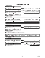
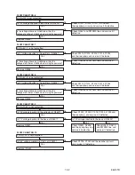


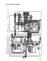
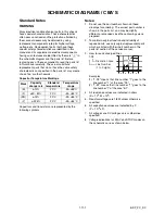
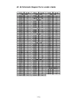
1-10-3
E5J10BLD2
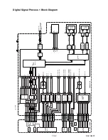
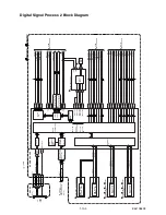
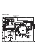
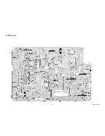
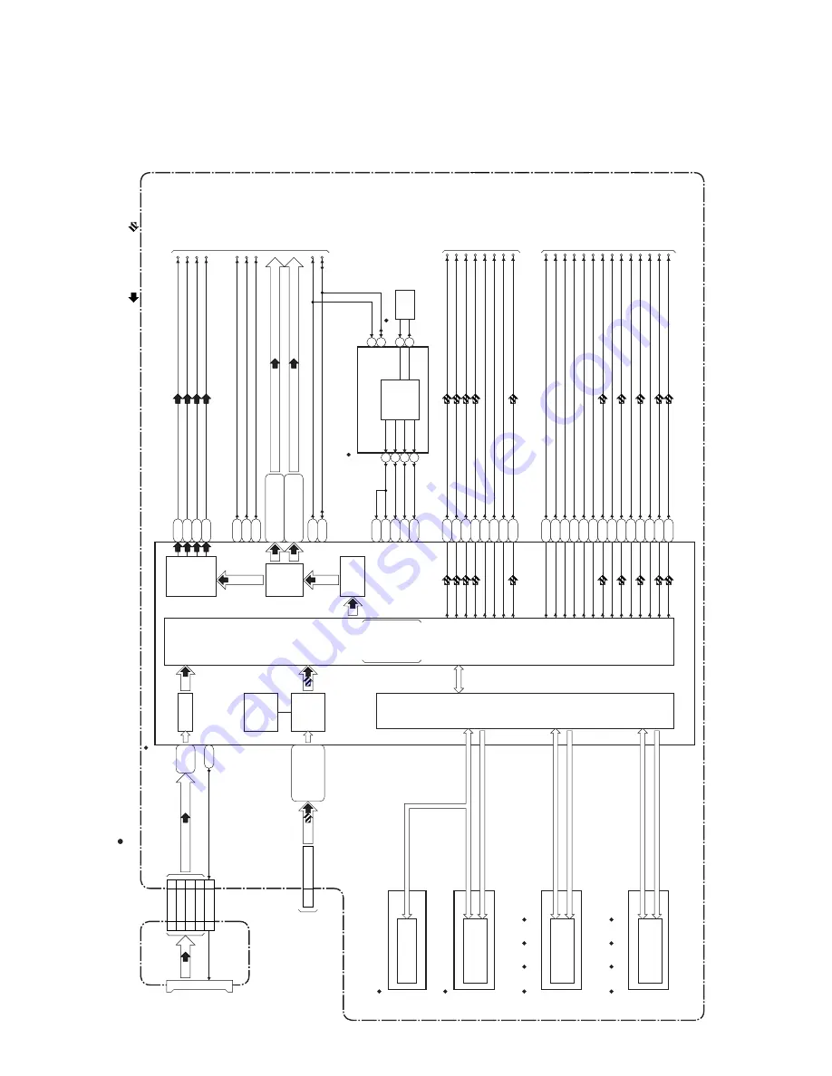
Digital Signal Process 2 Block Diagram
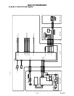
SD CB
A
BE MAIN CB
A UNIT
STREAM
CONTR
OL
A
T
A
PI I/F
ED (0-7)
ED (0-15)
ED (0-15)
EA (1-22)
C0DQ (0-31)
PC0A (0-12)
C1DQ (0-31)
PC1A (0-12)
MEDIA
PR
OCESSOR
J
a
v
a (BD-J)
MPEG-2
DECODER
HD (TS)
SD (PS)
COPY
PR
O
TECT
AA
CS
/BD+
SD
CARD
SLO
T
T
O
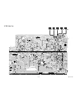
DIGIT
AL
SIGNAL PR
OCESS 1
BLOCK DIA
GRAM
(CN501)
CN4001
CN7602
CN6401
CN4002
MEMOR
Y
I/F
SD I/F
IC6001
(BE DIGIT
AL SIGNAL PR
OCESS)
IC6704
(CLOCK GENE.)
F25
A3
C14
C13
B14
IC6901
(NAND FLASH MEMOR
Y)
NAND FLASH
MEMOR
Y (64Mbit)
IC6902
(NOR FLASH MEMOR
Y)
(DDR SDRAM)
NOR FLASH
MEMOR
Y (8Mbit)
IC6501,IC6502,IC6503,IC6504
DDR SDRAM
(512Mbit x 4)
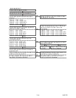
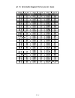
3-18
IDE1D(0-15)
13
13
SDD
A
T
0
15
15
SDD
A
T
1
11
SDD
A
T
2
33
SDD
A
T
3
11
11
SDCLK
(DDR SDRAM)
IC6507,IC6508,IC6509,IC6510
DDR SDRAM
(512Mbit x 4)
D33,D34,E32-E34,
F32-F34,G30,G32,
H29,H30,H32,
J28-J30
A8,A9,A11,B8,B10,B11,
C11,E12,E13,F14,G13,G14
A10,A12,A13,B9,B12,B13,
C10,C12,E14,F13,F15,G15
A27,B27,
F26,G26
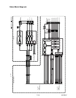
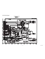
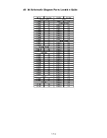
GRAPHICS
/OSD
PIXEL
D
A
T
A
I/F
VIDEO
DA
C
CLK
VS
HS
SD CLOCK
SD D
A
T
A(0-3)
T
O
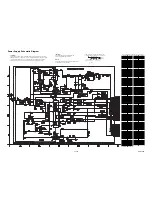
VIDEO
BLOCK DIA
GRAM
VIDEO
PRMCLK
PRMVS
PRMHS
PRMC(0-11)
PRMY(0-11)
SCL
33M CLOCK
33M CLOCK
74M CLOCK
27M CLOCK
768K CLOCK
SCL
SD
A
HDMI-D
A
T
A
0
HDMI-D
A
T
A
1
HDMI-D
A
T
A
2
HDMI-D
A
T
A
3
HDMI-MCK
HDMI-BCK
HDMI-LRCK
HDMI-SPDIF
X6701
27MHz
OSC
CLOCK
GENE.
SD
A
VIDEO-Y(I/P)
VIDEO-Pb/Cb
VIDEO-Pr/Cr
VIDEO SIGNAL
AUDIO SIGNAL
E9
C5
G9
SCL
B16
SD
A
C16
T
O
VIDEO
BLOCK DIA
G
RAM
E11
AP2
F11
D10
A6
C7
G11
B6
A5
2
3
1
16
7
8
9
10
F28
A31
B30
A28
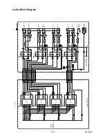
MC
MD
SCK
BCK
LRCK
MS3
D
ATA
1
MS4
D
ATA
2
MS2
D
ATA
0
MS1
D
ATA
SPDIF
T
O
A
U
DIO
BLOCK DIA
GRAM
G19
G20
L1
K5
K3
P32
K1
P29
L5
N34
L6
M34
K2
M7
“
“ = SMD
Summary of Contents for BDP7200/12
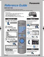
Page 10: ...1 4 1 E5J10IB OPERATING CONTROLS AND FUNCTIONS ...
Page 11: ...1 4 2 E5J10IB ...
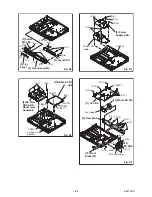
Page 40: ...AV CBA Top View BE5J10F01071A 1 11 9 ...
Page 56: ...BE Main 9 10 Schematic Diagram E5J10SCBM9 SMD 1 11 25 ...
Page 57: ...BE Main 10 10 Schematic Diagram E5J10SCBM10 SMD 1 11 26 ...
Page 58: ...BE Main CBA Top View 1 11 27 BE5E00G08016 ...
Page 59: ...BE Main CBA Bottom View 1 11 28 BE5E00G08016 ...
Page 62: ...FE Main 3 5 Schematic Diagram E5J10SCFM3 1 11 31 SMD ...