background image

Circuit Descriptions

EN 49

Q549.2E LA

7.

2009-May-08

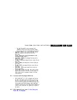
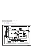
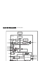
Figure 7-10 PNX8543 connectivity and compute subsystem

The Connectivity Subsystem consists of:

PCI/XIO interface

USB2.0 interface

Three 2-wire UARTs

Four Master/Slave I

2

C interfaces

Common Interface/Conditional Access Interface.

The Computing Subsystem consists of:

32-bit MIPS RISC core

Enhanced JTAG (EJTAG) block inside the MIPS

JTAG_MMIO blocks

TV  controller

Audio/Video DSP (AV_DSP)

Memory Control Unit (MCU).

7.5.4

Service Notice - FLASH RAM / PNX8543 exchange

The FLASH RAM (item 7P10) and/or PNX8543 (item 7H00) 
can only be exchanged by an authorised central workshop with 
dedicated programming tools. Due to the presence of (CI+) 

keys in the components, 

unauthorised exchange of these 

components will always result in a defective board

.

1

8

440_205_090226.ep

s

090226

JTAG_MMIO

UART2

UART1

IIC2_DMA

IIC

3

_DMA

MIP

S

4KEc

S

Y

S

TEM

CONTROLLER

8

0C51

PCI_XIO

CAI

MCU_DDR

DMA B

U

S

DC

S

-NETW

ORK

DDR2-

S

DRAM

I2C-2

I2C-

3

EJTAG

PNX

8

54

3

x

UART-1

UART-2

I2C-MC

UART-

3

PWM

s

GPIO

s

CI/CA

PCI/XIO

EJTAG

U

S

B2.0

U

S

B

AVD

S

P

IIC4_DMA

I2C-1

Summary of Contents for 32PFL9604H/12

Page 1: ...st 6 4 Mechanical Instructions 10 5 Service Modes Error Codes and Fault Finding 15 6 Alignments 36 7 Circuit Descriptions 42 8 IC Data Sheets 53 9 Block Diagrams Wiring Diagram 32 Elite Core 59 Wiring Diagram 37 Elite Core 60 Block Diagram Video 62 Block Diagram Audio 63 Block Diagram Control Clock Signals 64 Block Diagram I2C 65 SSB SRP List Part 2 136 Light guide 139 140 Wi Fi Antenna 141 141 ...

Page 2: ...cal Specifications 2 2 Directions for Use 2 3 Connections 2 4 Chassis Overview Notes Figures can deviate due to the different set executions Specifications are indicative subject to change 2 1 Technical Specifications For on line product support please use the links in Table 2 1 Here is product information available as well as getting started user manuals frequently asked questions and software dr...

Page 3: ...Technical Specifications and Connections EN 3 Q549 2E LA 2 2 3 Connections VGA SERVICE UART ...

Page 4: ... Connector jk Cinch S PDIF Out Bk Coaxial 0 4 0 6VPP 75 ohm kq Cinch Audio Out Rd Audio R 0 5 VRMS 10 kohm kq Wh Audio L 0 5 VRMS 10 kohm kq EXT3 Cinch Video YPbPr In Audio In Gn Video Y 1 VPP 75 ohm jq Bu Video Pb 0 7 VPP 75 ohm jq Rd Video Pr 0 7 VPP 75 ohm jq Rd Audio R 0 5 VRMS 10 kohm jq Wh Audio L 0 5 VRMS 10 kohm jq EXT1 2 Video RGB In CVBS In Out Audio In Out Figure 2 4 SCART connector 1 A...

Page 5: ...d H 3 D2 Data channel j 4 D1 Data channel j 5 Shield Gnd H 6 D1 Data channel j 7 D0 Data channel j 8 Shield Gnd H 9 D0 Data channel j 10 CLK Data channel j 11 Shield Gnd H 12 CLK Data channel j 13 Easylink CEC Control channel jk 14 n c 15 DDC_SCL DDC clock j 16 DDC_SDA DDC data jk 17 Ground Gnd H 18 5V j 19 HPD Hot Plug Detect j 20 Ground Gnd H 2 4 Chassis Overview Refer to chapter Block Diagrams ...

Page 6: ...erial connection on the set The reading should be between 4 5 MΩ and 12 MΩ 4 Switch off the set and remove the wire between the two pins of the Mains AC Power plug Check the cabinet for defects to prevent touching of any picture carrier at 475 25 MHz for PAL or 61 25 MHz for NTSC channel 3 Where necessary measure the waveforms and voltages with D and without E aerial signal Measure the voltages in...

Page 7: ...igit 3 refers to the B O M code digit 4 refers to the Service version change code digits 5 and 6 refer to the production year and digits 7 and 8 refer to production week in example below it is 2006 week 17 The 6 last digits contain the serial number 3 4 Abbreviation List 0 6 12 SCART switch control signal on A V board 0 loop through AUX to TV 6 play 16 9 format 12 play 4 3 format AARA Automatic As...

Page 8: ...TXT Green TeleteXT H H_sync to the module HD High Definition HDD Hard Disk Drive HDCP High bandwidth Digital Content uses 8 bit or 10 bit data words and has a maximum data rate of 270 Mbit s with a minimum bandwidth of 135 MHz ITV Institutional TeleVision TV sets for hotels hospitals etc LS Last Status The settings last chosen by the customer and read and stored in RAM or in the NVM They are calle...

Page 9: ...récepteurs et Téléviseurs SCL Serial Clock I2 C SCL F CLock Signal on Fast I2 C bus SD Standard Definition SDA Serial Data I2C SDA F DAta Signal on Fast I2 C bus SDI Serial Digital Interface see ITU 656 SDRAM Synchronous DRAM SECAM SEequence Couleur Avec Mémoire Color system mainly used in France and East Europe Color carriers 4 406250 MHz and 4 250000 MHz SIF Sound Intermediate Frequency SMPS Swi...

Page 10: ...structions Index of this chapter 4 1 Cable Dressing and Taping 4 2 Service Positions 4 3 Assy Panel Removal 4 4 Set Re assembly Notes Figures below can deviate slightly from the actual situation due to the different set executions 4 1 Cable Dressing and Taping ...

Page 11: ...Mechanical Instructions EN 11 Q549 2E LA 4 Figure 4 2 Cable dressing 37 18310_211_090318 eps 090318 ...

Page 12: ...hat the foam bars are always supporting the cabinet and never only the display Caution Failure to follow these guidelines can seriously damage the display By laying the TV face down on the ESD protective foam bars 4 3 3 Ambi Light Each Ambi Light unit is mounted on a subframe Refer to Figure 4 5 for details Figure 4 5 Ambi Light unit 1 Remove the Ambi Light cover 1 2 Unplug the connector s 3 The P...

Page 13: ...utions must be taken during removing or remounting Refer to Figure 4 7 Figure 4 8 and Figure 4 9 for details Figure 4 9 Piezo Touch Control Panel 3 1 To unplug the flexfoil connector first the outer part of the connector has to be moved upwards 3 before this part can be turned sidewards 4 as shown in the picture Now the flexfoil can be removed from the connector and the PWB can be taken out of the...

Page 14: ...Mechanical Instructions EN 14 Q549 2E LA 4 Figure 4 10 LCD Panel 1 18310_217_090318 eps 090320 1 4 1 18310_218_090318 eps 090319 3 2 ...

Page 15: ...r a hardware interface between a computer and the TV chassis It offers the abilities of structured troubleshooting error code reading and software version read out for all chassis see also section 5 4 1 ComPair Note For the new model range a new remote control RC is All service unfriendly modes if present are disabled like Sleep timer Child parental lock Picture mute blue mute or black mute Automa...

Page 16: ...planation see section 5 5 Error Codes Reset Error Buffer When cursor right or the OK button is pressed and then the OK button is pressed the error buffer is reset Alignments This will activate the ALIGNMENTS sub menu See Chapter 6 Alignments Dealer Options Extra features for the dealers TV will go to the Stand by mode If the NVM was corrupted or empty before this action it will be initialized firs...

Page 17: ...andard RC transmitter Note Activation of the CSM is only possible if there is no user menu on the screen NVM ComPair will foresee in a possibility to do this This identification number is the 12nc number of the SSB 12NC display Shows the 12NC of the display 12NC supply Shows the 12NC of the supply 12NC fan board Shows the 12NC of the fan board module for sets with LED backlight 12NC LED Dimming Pa...

Page 18: ...tion now The TV will stay in this situation until it is reset Mains AC Power supply interrupted Caution in case the start up in this mode with a faulty FET 7U08 is done you can destroy all IC s supplied by the 3V3 due to overvoltage 12V on 3V3 line It is recommended to measure first the FET 7U08 or others FET s on shortcircuit before activating SDM via the service pads The abbreviations SP and MP ...

Page 19: ...ed by the 1V2 DCDC converter No Detect 1 I O line High Switch ON Platform and display supply by switching LOW the Standby line This enables the 3V3 and 5V converter As a result also 5V tuner 2V5 1V8 PNX8541 and 1V8 PNX5100 become available yes Enable the DCDC converter for 3V3 and 5V ENABLE 3V3 Important remark the appearance of the 12V will start the 1V2 DCDC converter automatically No Yes Supply...

Page 20: ...onomously Wait 3000 ms Start alive IIC polling mechanism POR polling positive yes No Log SW event STi7100PorFailure Wait 200 ms POR polling positive yes No bootSTi7100PorFailure Log HW error Layer1 2 Layer2 38 and generate cold boot Alive polling Log SW event STi7100AliveFailedError and generate fast cold reboot eventually followed by a cold reboot NOK Reset system is switched HIGH by the AVC at t...

Page 21: ...to account Display may only be started when valid LVDS output clock can be delivered by the AVC Between 5 and 50 ms after power is supplied display should receive valid lvds clock minimum wait time to switch on the lamp after power up is200ms Wait until valid and stable audio and video corresponding to the requested output is delivered by the AVC The higher level requirement is that audio and vide...

Page 22: ...vds clock minimum wait time to switch on the lamp after power up is200ms To have a reliable operation of the backlight the backlight should be driven with a PWM duty cycle of 100 during the first second Only after this first one or two seconds the PWM may be set to the required output level Note that the PWM output should be present before the backlight is switched on To minimize the artefacts the...

Page 23: ...nly be started when valid LVDS output clock can be delivered by the AVC Between 5 and 50 ms after power is supplied display should receive valid lvds clock minimum wait time to switch on the lamp after power up is200ms Wait until valid and stable audio and video corresponding to the requested output is delivered by the AVC The higher level requirement is that audio and video should be demuted with...

Page 24: ...dio outputs to ground I O audio reset And wait 5ms Switch off the display by sending the TurnOnDisplay 0 I C command to the PNX5100 switch off Ambilight Set main amplifier mute I O audio mute Wait 100ms Wait until Ambilight has faded out fixed wait time of x s The higher level requirement is that the backlight may not be switched off before the ambilight functionality is turned off in case the set...

Page 25: ... ST7100 LOW Switch Reset Ethernet LOW Important remark release reset audio 10 sec after Wait 5ms Wait 10ms Switch the NVM reset line HIGH Switch het WP Nandflash LOW Delay transition until ramping down of ambient light is finished If ambientlight functionality was used in semi standby lampadaire mode switch off ambient light If this is not performed and the set is switched to standby when the swit...

Page 26: ...nter protection state SP Switch off LCD lamp supply Wait 250ms min 200ms Switch off LVDS signal Switch off 12V LCD supply within a time frame of min 0 5ms to max 50ms after LVDS switch off If needed to speed up this transition this block could be omitted This is depending on the outcome of the safety investigations Disable all supply related protections and switch off the 1V8 and the 3V3 DC DC con...

Page 27: ...o Test With this tool you can test the memory of the PNX8543 as well if the PNX5100 is enabled and audio testing What is needed An USB stick TESTSCRIPT Q549 Downloadable from the Philips Service website from the section Software for Service only A ComPair service cable 3138 188 75051 Procedure Create a directory JETTFILES under the root of the USB stick Place MemTestTV543 bin and autojett bin avai...

Page 28: ...D LAYER 1 error see section 5 6 The Blinking LED Procedure Errors detected by the Stand by software which not lead to protection In this case the front LED should blink the involved error See also section 5 5 Error Codes 5 5 4 Error Buffer Extra Info Note that it can take up several minutes before the TV starts blinking the error e g LAYER 1 error 2 LAYER 2 error 15 or 53 Errors detected by main s...

Page 29: ... a ComPair interface and Hyperterminal for Hyperterminal settings see section 5 8 Fault Finding and Repair Tips 5 8 6 Description Layer 1 Layer 2 Monitored by Error Prot Error Buffer Blinking LED Device Defective Board I2 C3 2 13 MIPS E BL EB SSB SSB I2 C2 2 14 MIPS E BL EB SSB Display SSB display PNX doesn t boot HW cause PNX 5100 doesn t boot 2 15 Stby µP P BL PNX8543 PNX51XX I2 C blocked SSB 12...

Page 30: ...ins is activated This is especially useful for fault finding and gives more details regarding the failure of the defective board Activate the CSM The blinking front LED will show only the latest layer 1 error this works in normal operation mode or automatically when the error protection is monitored by the standby processor In case no picture is shown and there is no LED blinking read the logging ...

Page 31: ...ely when 12V incoming voltage is available 12V is enabled by STANDBY signal active low Supply voltages 3V3 2V5 1V8 PNX5100 1V8 PNX85XX 5V and 5V TUN are switched on directly by signal ENABLE 3V3 active low provided that 12V detected via 7U40 7U41 is available 12V is considered OK DETECT 12V signal becomes high and 12V 3V3 and 12V 5V DC DC converter can be started up if it rises above 10V5 typical ...

Page 32: ... tuner is replaced always check the tuner options 5 8 10 PCI bus The splash screen image is not distributed via the regular YUV signal path from the PNX8543 to the PNX51XX but loaded one time via the PCI bus Once the splash screen image is loaded into the PNX51XX it will be continuously generated by the PNX51XX until the first incoming video disables the splash screen So when teletext and or gener...

Page 33: ...522 x Q529 x Q54x x Set is starting up but no display Update main software in this step by using autorun upg file Noisy picture with bands lines is visible and the red LED is continuous on sometimes also the letter F is visible Press 5 s the Volume minus button on the local cntrl until the red LED switches off and then press 5 s the MENU button of the local cntrl in some chassis this button is nam...

Page 34: ...consumers themselves but they will have to get their software from the commercial Philips website or via the Software Update Assistant in the user menu see eUM The 5 The renamed upg file will be visible and selectable in the upgrade application Back up Software Upgrade Application If the default software upgrade application does not start could be due to a corrupted boot 2 sector via the above des...

Page 35: ... zip Not to be used by Service technicians LightGuide_TV522_x x x x_ zip Not to be used by Service Technicians ProcessNVM_Q5492_x x x x zip Default NVM content Must be programmed via ComPair or can be loaded via USB be aware that all alignments stored in NVM are overwritten here 5 9 5 Content of the MOP Ambilight ARM SW File MOP_AMBILIGHT_V1 2_UPG_jettsigned zip Contains the MOP ambientlight softw...

Page 36: ...rding to the set sticker see also paragraph 6 4 Option Settings Press OK on the remote control before the cursor is moved to the left In submenu Option numbers select Store and press EU AP PAL models a PAL B G TV signal with a signal strength of at least 1 mV and a frequency of 475 25 MHz US AP NTSC models an NTSC M N TV signal with a signal strength of at least 1 mV and a frequency of 61 25 MHz c...

Page 37: ... display code overview for the options Diversity Not all sets with the same Commercial Type Number CTN necessarily have the same option code Use of Alternative BOM an alternative BOM number usually indicates the use of an alternative display or power supply This results in another display code thus in another Option code For the power supply there is no difference Refer to Chapter 2 Technical Spec...

Page 38: ...ere xxx is the 3 digit display panel code see sticker on the side bottom of the cabinet 6 6 2 When no picture is available Due to a possible wrong display option code in the received Service SSB NVM no picture can be available at start up and thus no download application will be visible Here you can proceed and finalize step by step to load the main TV software via the UART logging on the PC for v...

Page 39: ...hernet Off On Select Ethernet On Off Wi Fi Off On Select Wi Fi On Off DLNA Off On Select DLNA On Off Online service Off Online service is Off PTP Picture Transfer Protocol Off On Select PTP On Off Update assistant Off On Select Update assistant On Off Internet software update Off Internet software update is Off Display Screen 180 LCD Sharp Z3LA13 56 Displayed the panel code type model LightGuide O...

Page 40: ...lect HDMI side On Off HDMI CEC Off On Select HDMI CEC On Off HDMI CEC RC passthrough Off On Select HDMI CEC RC passthrough On Off HDMI CEC Pixel Plus link Off On Select Pixel Plus link On Off Miscellaneous Region Europe AP PAL MULTI Australia Select Region country Tuner type HD1816 MK1 TD1716 MK4 TD1716 MK3 HD1816 MK2 Select type of Tuner used System RC support Off On Select System RC support On O...

Page 41: ...zip software Display information is for development purposes Initial main software NVM version Q5492_0 4 0 0 Flash units SW Q5492_0 26 15 0 Upload to USB Channel list To upload several settings from the TV to an USB stick Personal settings Option codes Display related alignment History list Download from USB Channel list To download several settings from the USB stick to the TV Personal settings O...

Page 42: ...Introduction The Q549 2E LA chassis platform name TV543 92 is the successor of the Q529 1E LA chassis platform TV522 92 Main difference with the previous platform is the introduction of Net TV and CI 7 1 1 Implementation Key components of this chassis are PNX8543 Digital Colour Decoder EP3C25F324C7N FPGA Local Contrast HD1816AF Hybrid Tuner DRX3926K Demodulator TDA9996 HDMI Switch TPA3123D2PWP Cla...

Page 43: ...59 1M20 1M01 1R12 1M36 TDA 98XX Class D 1R08 1R07 1HP0 1CJ0 Xilinx Pr Pb L Lo Y Ro Scart YPbPr TDA 10048 TDA 10023 1 7 3 5 H D M I 1M95 1 H 0 1 DDR2 DDR2 PNX8542 3 Video In Video Out DV in TS in HDMI B HDMI A PCI CA DDR LVDS 2 LVDS 1 USB Audio In Audio Out E J T A G STBY GPIO DDR Ethernet FLASH HDMI MUX 1E51 1E50 1G50 1G51 Wifi L R 1HE0 CY3 C40 H D M I RJ45 5100 40x40 1 27 DDR2 GPI O lvds rx ambi ...

Page 44: ...DC DC 2 5V 1 voltage ref 2V5 2V5 1V8 1V8 3V3F 5V 5V tuner 5V Tun PNX5100 1V2 PNX85XX 5V 3V3 1V8 PNX5100 1V8 PNX85XX 2V5 loc Contr FPGA 1V2 PNX 5100 5V TU N SSB Bolt on V inverter 4kV Inverter Lamp On BL DIM Lamp On BL DIM Inverter Stby P Enable 3V3 12V U ndervoltage detect Sw itches off 3V3 and 5V present in inverterless displays present in displays with internal inverter D etect 2 12V sense AN D ...

Page 45: ...EDID contents are at 5V power up downloaded to RAM The following figures show the HDMI input configuration and EDID control Figure 7 6 EDID control embedded EDID The delta s with respect to the use of the TDA9996 as HDMI multiplexer compared with earlier chassis platforms are 5V detection mechanism Stable clock detection mechanism Integrated EDID RT control HPD control TMDS output control CEC cont...

Page 46: ...AUDIO DSP AUDIO DACS AUDIO OUT 300 MHz 300 MHz I2C PWM GPIO IR ADC UART I2C GPIO Flash SYSTEM USB 2 0 CA PNX8543x DV INPUT DV ITU 656 AV PIP SPI MPEG H 264 I2S RECEIVER 8051 CONTROLLER AND DECODE DECODER channel decoder PCMCIA RGB PROCESSOR SYSTEM CONTROLLER DECODER VIDEO CPU MIPS32 4KEc 0 1 x 2 2 x AV DSP REDUCTION AND NOISE DE INTERLACE OUTPUT VIDEO SUB PICTURE ENCODER OUTPUT VIDEO channel singl...

Page 47: ...R DMA BUS DDR2 SDRAM PNX8543x VCP_ UIP DENC DAC VCP_ WIFD HDMI_ RX MBVP_ L2VO2 MBVP_ L2QTV MBVP_ L2VO1 A A GFX2 PIP CVBS1 Y monitor main CVBS2 C monitor HDMI VCP PC LOW IF CVBS RGB Dual HDMI FPD LVDS1 LCD panel MUX VCP_RX 2D_DE VIP ITU 656 PC_ UIP GFX1 FPD LVDS2 LCD panel CVBS Y C CAI TS TSDO TSDI CMD PCMCIA TSI MSVD DV including ITU 656 YPbPr VGA ...

Page 48: ...0 MPEG AC 3 MP3 DECODER SPDIF OUT AO AI APP AUDIO DSP POST PROCESSING DMA BUS I2S OUT SD3 I2S OUT SD4 I2S OUT WS I2S OUT SCK I2S OUT OSC HDMI SPDIF IN1 IF SSIF TS IN SPDIF Out SPDIF IN2 I2S OUT SD1 I2S OUT SD2 I2S IN SD3 I2S IN SD4 I2S IN WS I2S IN SCK I2S IN OSC I2S IN SD1 I2S IN SD2 SPDIF 4 4 I2S 4 4 I2S XB3 XB4 from XB4 fast SPDIF XB1 XB2 4 I2S ...

Page 49: ...ns EN 49 Q549 2E LA 7 UART2 UART1 IIC2_DMA IIC3_DMA MIPS 4KEc SYSTEM PCI_XIO CAI MCU_DDR DMA BUS DCS NETWORK DDR2 SDRAM I2C 2 I2C 3 PNX8543x UART 1 UART 2 I2C MC UART 3 CI CA PCI XIO EJTAG USB2 0 USB AVDSP IIC4_DMA I2C 1 ...

Page 50: ...ule CAM and the Integrated Digital Television IDTV The security mechanisms in CI are derived copied from POD with the exception of Out Of Band OOB used in US CA systems For more information about conventional CA systems using a CI module refer to the BJ3 0E L PA or BL2 xU Service Manual The CI standard is downwards compatible with the existing CI standard The following figure shows the implementat...

Page 51: ...ration operation mode and topology data via I2 C The controller converts the I2 C RGB data via the matrixes to SPI LED data Via data return the controller receives error data if applicable Also PWM clock and BLANK signals are generated by the controller The controller can be reprogrammed via I2 C via USB The controller can receive matrix values via I2 C which will be stored in the EEPROM of each A...

Page 52: ...RN is linked from the last driver to the controller controller decides which driver returns data 7 8 3 Temperature Control Refer to Figure 7 15 for signal interfacing between the ARM controller and the temperature sensor on the AL boards Figure 7 15 Communication between ARM controller and temperature sensor Each AL board is equipped with a temperature sensor If one of the sensors detects a temper...

Page 53: ... Sheets This chapter shows the internal block diagrams and pin configurations of ICs that are drawn as black boxes in the electrical diagrams with the exception of memory and logic ICs 8 1 Diagram SSB DC DC B01A TPS53124PW IC 7U03 Block Diagram ...

Page 54: ...System Controller SAW Main Tuner Presaw Sense DVB T QAM FEC DAC DAC MPEG 2 TS CVBS SIF I2S Audio I2 C GPIO IF AGC RF AGC Integrated Tuner I2C ADC IF AMP 49 XI 50 XO RSTN 32 SAW_SW 31 PDP VDDAL_AFE2 VSSAL_AFE2 SIF CVBS VDDAH_CVBS VSSAH_CVBS PDN INP INN VSSAH_AFE1 VDDAH_AFE1 VDDAL_AFE1 VSSAL_AFE1 IF_AGC RF_AGC 48 47 46 45 44 43 42 41 40 39 38 37 36 35 34 33 ...

Page 55: ... DIGITAL IF AUDIO DEMOD AUDIO IN HDMI SCALER AUDIO DSP AUDIO DACS AUDIO OUT 300 MHz 300 MHz I2C PWM GPIO IR ADC UART I2C GPIO Flash SYSTEM USB 2 0 CA PNX8543x DV INPUT DV ITU 656 AV PIP SPI MPEG H 264 I2S RECEIVER 8051 CONTROLLER AND DECODE DECODER channel decoder PCMCIA RGB PROCESSOR SYSTEM CONTROLLER DECODER VIDEO CPU MIPS32 4KEc 0 1 x 2 2 x AV DSP REDUCTION AND NOISE DE INTERLACE OUTPUT VIDEO S...

Page 56: ...0 Pin Configuration Block Diagram LVDS RX 1 UIP L3K7 TM327x 1 CONTROLLER PCI XIO I2C DMA UART CPIPE L3K7 LVDS TX 2 UART PNX51xx I2C I2C TM327x 2 TM327x 3 LVDS TX 3 LVDS TX 1 LVDS TX 4 GFX 16 X GPIO GIC 3 EJTAG CLOCK CAB Video LVDS RX 2 AUDIO IN AUDIO OUT GIC 1 GIC 2 MEMORY Video ...

Page 57: ...3 112 110 109 111 N L E S V E D N Y D R T N Y D R I N E M A R F 2 N E B C 6 1 D A 7 1 D A 8 1 D A N P O T S N R R E P N R R E S R A P 1 N E B C 5 1 D A 4 1 D A 3 1 D A 2 1 D A 1 1 D A 0 1 D A AD9 S S V AD8 9 1 D A 0 2 D A 1 2 D A 2 2 D A 3 2 D A L E S D I S S V D D V I C P C N D D V I C P C N S S V D D V I C P 3 N E B C 4 2 D A 5 2 D A AD26 CBEN0 VSS AUXVDD RESERVED VREF PCIVDD AD29 AD31 VSS REQN ...

Page 58: ...PVCCR VCLAMP GAIN1 BYPASS 1 F 1 F 0 22 F AGND Control Shutdown Control LIN RIN BSR BSL PGNDR PGNDL 0 22 F 22 H 22 H 0 68 F 470 F 0 68 F 1 F 470 F GAIN0 AVCC MUTE ROUT LOUT 1 2 3 4 5 6 7 8 9 10 24 23 22 21 20 19 18 17 16 15 PVCCL SD PVCCL MUTE LIN RIN BYPASS AGND AGND PVCCR PGNDL PGNDL LOUT BSL AVCC AVCC GAIN0 GAIN1 BSR ROUT ...

Page 59: ...B 12 GND 11 SDA SET 10 SCL SET 9 POWER OK 8 BACKLIGHT PWM 7 BACKLIGHT BOOST 6 BACKLIGHT OUT 5 LAMP ON OUT 4 GND 3 GND 2 12VD 1 12VD 1735 B10A 4 RIGHT SPEAKER 3 GND AUDIO 2 GND AUDIO 1 LEFT SPEAKER 1G50 B05C 41 N C 40 TXDAT 39 TXDAT 3 TX2E 2 SCL DISP 1 SDA DISP 1G51 B05C 51 N C 50 SDA DISP 49 SCL DISP 3 VDISP1 2 VDISP1 1 VDISP1 1M95 B01B 11 N C 10 GND 9 AUDIO POWER 8 12V 7 12V 6 12V 5 GND 4 GND 3 G...

Page 60: ... VDISP1 1 VDISP1 1M95 B01B 11 N C 10 GND 9 AUDIO POWER 8 12V 7 12V 6 12V 5 GND 4 GND 3 GND 2 STANDBY 1 3V3 STANDBY CN7 6 GND 5 24V 4 GND 3 24V 2 GND 1 24V WIFI ANTENNA 1044 WIFI ANTENNA 1043 WIFI MODULE ON 1A01 1042 1M84 AL1 14 GND 13 VLED2 12 GND 11 VLED1 10 PROG 9 TEMP SENSOR 8 EEPROM CS 7 BLANK BU 6 3V3 5 PWM CLOCK BUF 4 SPI LATCH 3 SPI DATA RETURN 2 SPI DATA OUT 1 SPI CLOCK BUF 1M84 AL1 14 GND...

Page 61: ...GND 8395 8399 8735 8319 8802 8150 8151 8735 8120 Board Level Repair Component Level Repair Only For Authorized Workshop KEYBOARD CONTROL 1127 1M01 3P 1A01 124P 1M90 AB1 6 GND 5 24V 4 GND 3 24V 2 GND 1 24V 1M59 AB1 7 GND 6 3V3 5 CONTROL2 4 CONTROL1 3 SDA 2 GND 1 SCL DC DC INTERFACE 1028 AB 8159 8690 1M84 AB1 14 GND 13 VLED2 12 GND 11 VLED1 10 PROG 9 TEMP SENSOR 8 EEPROM CS 7 BLANK BUF 6 3V3 5 PWM C...

Page 62: ...001CLK AC19 M2 TXF1CLK RX51001CLK AD19 M1 TXF1C RX51001C AE19 L2 TXF1C RX51001C AF19 L1 TXF1D RX51001D AE18 P2 TXF1D RX51001D AF18 P1 TXF1E RX51001E AC18 T3 TXF1E RX51001E AD18 R3 TXF2A RX51002A AE17 U2 TXF2A RX51002A AF17 V3 TXF2B RX51002B AC17 U4 TXF2B RX51002B AD17 V4 TXF2CLK RX51002CLK AC16 U6 TXF2CLK RX5100CCLK AD16 V6 TXF2C RX51002C AE16 U5 TXF2C RX51002C AF16 V5 TXF2D RX51002D AE15 U7 TXF2D...

Page 63: ...SET AUDIO AD1 AC5 ADAC 4 AUDIO HDPH L AP AUDIO HDPH R AP ADAC 3 Headphone Out 3 5mm AM12 AM11 7HV0 TPA6111A2DGN HEADPHONE AMPLIFIER 1 7 2 6 5 RESET AUDIO A PLOP B08A 7D10 TPA3123D2PWP CLASS D POWER AMPLIFIER OUT L OUT R 5 6 22 15 IN R IN L MUTE SD AUDIO MUTE 4 2 A STBY A STBY B08B STANDBY PROTECTION 7D03 LEFT SPEAKER RIGHT SPEAKER AUDIO IN5 L AUDIO IN5 R AL9 AL8 AN7 AP7 AK6 AL6 AP6 AM5 AN5 AP5 1E1...

Page 64: ... C10 B9 AB33 J8 K8 7N13 7N11 7N12 CA DATADIR CA ADDEN CA DATAEN CA MICLK H32 D31 A31 B31 TO POWER SUPPLY B08A AH2 AV2 BLK B08A 32 COMMON INTERFACE 1A01 1 68 MINI PCI CONNECTOR 7P15 7P16 USB OC TO POWER SUPPLY 3V3 STANDBY 5V B04M B01B B01C AD4 DETECT1 DETECT2 B04A B01B 9H25 9H13 3HFG 7 XIO ACK 9 XIO SEL NAND 18310_404_090305 eps 090327 A20 B20 L32 L31 UART SERVICE CONNECTOR UP STANDBY RES RES RXD U...

Page 65: ...MP SENSOR UART SERVICE CONNECTOR 3U67 3U66 3V3 3FA6 3FA5 3CDA 3CD9 TO AMBI LIGHT MODULE 9F22 9F21 3V3 3FAA 3FAB 3V3 3F37 3F36 3V3 1M59 3 4 5 7 1 3 EF 7HC4 I2C SDA I2C SCL 61 62 TUN P7 TUN P6 3T61 3T59 3V3 TUN SDA TUN SCL RXD UP TXD UP RXD TXD 13 14 2 9 1 4 11 8 RXD MIPS TXD MIPS RXD UP TXD UP D15 C15 DDC_SDA_B M_DQ M_A DDC_SCL_B DDC SDA DDC SCL 9FA2 9FA1 9F20 9F19 9F15 9F13 5F05 SDA AMBI 3V3 SCL A...

Page 66: ...O 5HY7 AUDIO ADC 5HY4 VDDA DAC 1V2 PNX85XX 1V2 PNX85XX 3V3 STANDBY 3V3 STANDBY 1V2 STANDBY 1V2 STANDBY 3V3 3V3 5HVH 3V3 PER RREF PNX85xx 5HV8 1V8 PNX5100 1V8 PNX5100 PNX5100 DDR2 VREF CTRL PNX5100 DDR2 VREF DDR 3V3 3V3 3V3 3V3 3V3 PNX5100 LVDS PLL 5C70 VDISP2 VDISP2 3V3 3V3 3V3 3V3 VDDA DAC VDDA DAC 3C20 3C22 1G50 41 1V8 PNX5100 1V8 PNX5100 3V3 3V3 3V3 3V3 AUDIO POWER AUDIO POWER ADIO VDD AUDIO VD...

Page 67: ... D 9 A B 10 J 11 9101 C3 9102 C3 9103 C3 9104 C3 F101 B3 F102 B3 F103 B3 F104 B3 F105 B3 F106 B3 F107 A7 F108 B3 F111 B3 F112 B3 F113 B3 A 5 4 F VLED1 12V RES 16V F118 5101 30R VSW I108 F103 3V3 24VF F112 I100 12V RES 100R 3109 4 5 6 7 1735446 7 1M59 1 2 3 24V F107 RES 9103 I106 3K3 3108 1 3102 15K 2102 F101 2n2 F104 5106 30R 16V 16V F122 9104 1 SUPERS 1 NAME DATE MGr CHECK 3104 313 6325 AMBI 2K9 ...

Page 68: ...dc dc converter A B 12 5 H 3212 D6 3213 D6 5200 B2 5201 B7 4 E 11 22u 2209 RES 2200 A4 2201 A4 2202 A5 2203 A5 2204 B3 2205 B6 2206 B1 E The components marked with one star belong to the 12V versions 3104 328 58351 3104 328 58371 2221 D3 2222 D5 2223 D8 2224 D8 3204 10R 33K 3213 I201 3207 68K 9202 1 I217 100u 2206 F202 35V 3208 47K 1 4u7 2207 RES 12V 2208 22u F200 I214 F207 I209 2200 100u 35V 12V ...

Page 69: ...0 3 10K 3 3327 10K 1V8 3V3 10K RES 3326 10K 3302 4 4 5 1 8 F310 2 7 100R 3308 1 3 4 5 3308 2 100R 1302 B3B PH SM4 TBT LF 1 2 3V3 RES 3313 10K 8 2303 10n 3301 1 10K 1 I308 I304 I319 I313 1 1K5 3311 5 4 3104 313 6325 AMBI 2K9 DC DC INTERFACE A2 08 08 06 08 06 19 08 12 06 08 10 23 08 09 18 08 08 06 5 4 3 2 130 3309 4 100R 3 2 08 10 23 Peter Van Hove 08 06 19 ROYAL PHILIPS ELECTRONICS N V 2008 08 06 0...

Page 70: ...1 3202 3203 3204 3205 3206 3207 3208 3209 3210 3211 3212 3213 3300 3301 3302 3303 3304 3305 3310 3311 3312 3313 3314 3315 3316 3317 3318 3319 3320 3321 3322 3323 3325 3327 3328 3329 3330 3332 3333 3334 3335 3336 3337 3339 5100 5101 5103 5104 5105 5106 5107 5108 6100 7100 7300 7302 7303 9300 9301 9302 9303 9305 9307 C300 F101 F102 F103 F104 F105 F106 F107 F108 F109 F110 F111 F112 F113 F114 F115 F11...

Page 71: ...37 F108 3125 1 100R 2115 100p 16 14 2 3 4 5 6 7 8 9 15 1 10 11 12 13 F138 1M83 5 F102 3105 4 10K 4 REF EMC HOLE 1X03 1 2 3 4 5 F123 F121 2113 100n 10K 3103 2 2 7 3102 3 3 6 10K 3137 RES F131 10K F126 2 7 9102 1 8 3124 2 100R 3V3 10K 3102 1 F101 I125 2130 1u0 9119 3130 22R 2108 10n 3109 100R 2110 100p 3117 10K 1 8 10K 2111 100n 3106 1 VLED2 RES 10K 3108 10K 3114 3118 RES 10K VLED1 F127 3V3 2128 10u...

Page 72: ... is prohibited without the written consent of the copyright F 9 10 11 12 13 1 2 3 4 5 6 D 3 2 8 1 2 16 9 19 4 15 K G 1 2 3 4 5 6 7 8 13 C 14 3 G E E owner 5 H 14 G H I 2201 B8 2202 C8 2203 D8 2209 B2 2210 G6 2211 I6 2214 A6 2215 F7 2216 F7 9 D 6 15 13 19 5 I 17 MICROCONTROLLER LITEON M 10 B RES 3207 1K0 1u0 2216 F202 10K 3210 3V3 33p 2209 6216 SML 310 2211 33p 9212 3V3 RES 100R 3121 3220 3223 100R...

Page 73: ...8 I O 3364 F13 15 3327 H4 3330 I4 3331 F4 3332 F4 A J D 3372 F1 3338 D1 3339 D2 3340 D1 I A B 3344 D1 3389 F1 3346 E1 16 7000 C2 F F 8 H 3347 D1 13 20 12 F G 2 17 3315 E12 3316 E12 3317 F12 7 8 9 3321 G12 3353 E1 3323 G12 N 3356 E1 B LED LITEON 8 K if VLED 17V 15 14 3328 G4 13 G B D M 3337 D2 F G H 4 5 6 C 3345 D12 E 17 10 11 19 3305 G9 3306 H9 3307 H9 D R P 5 E O 3 3314 E12 4 5 6 C 4 10 3322 G12 ...

Page 74: ...8 3330 3331 3332 3333 3334 3335 3336 3337 3338 3339 3340 3341 3342 3343 3344 3345 3346 3347 3348 3349 3350 3351 3352 3353 3354 3355 3356 3357 3358 3359 3360 3361 3362 3363 3364 3365 3366 3367 3368 3369 3370 3371 3372 3373 3374 3384 3385 3386 3387 3388 3389 3390 3391 6216 7000 7001 7002 7003 7004 7005 7101 7102 7110 7116 7201 7209 7210 7212 7214 7215 7305 7306 7307 7315 7316 7317 9101 9102 9103 910...

Page 75: ...3 4 42 5 17 40 7 19 43 31 11 23 P0 5 MISO0 MAT0 1 24 P0 6 MOSI0 CAP0 2 28 P0 7 SSEL0 MAT2 0 29 P0 8 TXD1 MAT2 1 30 P0 9 RXD1 MAT2 2 6 26 20 25 8 P0 27 TRST CAP2 0 9 P0 28 TMS CAP2 1 10 P0 29 TCK CAP2 2 18 P0 2 SCL0 CAP0 0 15 P0 30 TDI MAT3 3 16 P0 31 TDO 21 P0 3 SDA0 MAT0 0 22 P0 4 SCK0 CAP0 1 14 P0 1 RXD0 MAT3 2 2 P0 20 MAT1 3 MOSI1 3 P0 21 SSEL1 MAT3 0 32 P0 22 AD0 0 33 P0 23 AD0 1 34 P0 24 AD0 ...

Page 76: ...0K 3213 100p 2219 3V3 RES 8204 000 8857 3104 313 6314 3 2K9 DRIVER 6LED LITEON A2 2008 08 08 2008 08 08 3 2 130 2220 100p 3 2 Peter Van Hove 2008 06 10 ROYAL PHILIPS ELECTRONICS N V 2008 2008 06 02 2 3 SETNAME CHN CLASS_NO SUPERS 1 NAME DATE CHECK RES F203 3218 1K2 7210 PDTC144EU 1 3 2 2203 33p 9210 RES F214 9211 RES 3V3 9214 9209 28 30 31 32 33 23 26 3 11 12 13 14 15 16 4 5 24 6 7 8 17 18 19 20 2...

Page 77: ... 9315 2 C12 9315 4 C12 9312 3 B10 9312 4 B10 3360 E13 9306 1 D5 9306 3 D5 9306 4 D5 560R 3359 F349 VLED1 F 9316 3332 10K 9312 1 1 8 560R 3365 F305 BC847BW 7305 9302 3386 1K5 F304 1K5 3310 F347 390R 3351 3319 1K5 10K 3307 F341 F340 1K5 F344 3318 4 5 1K5 3350 9313 4 560R 3361 3330 10K 560R 3367 3347 1K5 4 5 3 6 9309 4 3352 9319 3 3355 560R 560R 560R 3371 1K5 3314 2 9309 1 1 8 1 6 4 3 7 5 F343 LTW E5...

Page 78: ...NAME CHN CLASS_NO 1 SUPERS 1 NAME DATE CHECK 8204 000 8874 3104 313 6314 3 2K9 2LED CONNECTOR A2 2008 08 08 2008 05 23 0 2008 08 08 3 2 2008 10 31 Peter Van Hove 2008 05 23 560R 3572 3571 560R 1K5 3586 3537 VLED1 390R 1K5 3547 3V3 1 6 4 3 7 5 2 3589 1K5 LTW E500T PH1 7006 3544 1K5 3553 560R 3555 1K5 VLED2 7 5 2 3V3 7007 LTW E500T PH1 1 6 4 3 390R 3539 560R 3573 3585 1K5 3543 560R VLED2 1X04 REF EM...

Page 79: ...3346 3347 3348 3349 3350 3351 3352 3353 3354 3355 3356 3357 3358 3359 3360 3361 3362 3363 3364 3365 3366 3367 3368 3369 3370 3371 3372 3373 3374 3384 3385 3386 3387 3388 3389 3390 3391 3536 3537 3538 3539 3540 3541 3542 3543 3544 3546 3547 3549 3550 3552 3553 3555 3556 3569 3570 3571 3572 3573 3574 3584 3585 3586 3587 3588 3589 3590 3591 6216 7000 7001 7002 7003 7004 7005 7006 7007 7101 7102 7110 ...

Page 80: ...3 I111 F133 5 9114 3125 4 100R 4 F112 100p 3105 1 10K 1 8 2117 12 3V3 4 42 5 17 40 7 19 43 31 11 23 P0 5 MISO0 MAT0 1 24 P0 6 MOSI0 CAP0 2 28 P0 7 SSEL0 MAT2 0 29 P0 8 TXD1 MAT2 1 30 P0 9 RXD1 MAT2 2 6 26 20 25 8 P0 27 TRST CAP2 0 9 P0 28 TMS CAP2 1 10 P0 29 TCK CAP2 2 18 P0 2 SCL0 CAP0 0 15 P0 30 TDI MAT3 3 16 P0 31 TDO 21 P0 3 SDA0 MAT0 0 22 P0 4 SCK0 CAP0 1 14 P0 1 RXD0 MAT3 2 2 P0 20 MAT1 3 MO...

Page 81: ...205 RES F206 3V3 1K0 3211 F215 3V3 9208 RES 3V3 2210 33p 2214 100n 10K 3213 100p 2219 3V3 RES 8204 000 8857 2K9 DRIVER 6LED LITEON A2 2008 08 08 2008 08 08 3 2 130 2220 100p 3 2 Peter Van Hove 2008 06 10 ROYAL PHILIPS ELECTRONICS N V 2008 2008 06 02 2 3 SETNAME CHN CLASS_NO SUPERS 1 NAME DATE CHECK RES F203 3218 1K2 7210 PDTC144EU 1 3 2 2203 33p 9210 RES F214 9211 RES 3V3 9214 9209 28 30 31 32 33 ...

Page 82: ...F346 D13 F342 D1 9304 4 E10 9305 1 C6 9305 2 C6 9305 4 C6 9315 1 C12 9315 2 C12 9315 4 C12 9312 3 B10 9312 4 B10 3360 E13 9306 1 D5 9306 3 D5 9306 4 D5 560R 3359 F349 VLED1 F 9316 3332 10K 9312 1 1 8 560R 3365 F305 BC847BW 7305 9302 3386 1K5 F304 1K5 3310 F347 390R 3351 3319 1K5 10K 3307 F341 F340 1K5 F344 3318 4 5 1K5 3350 9313 4 560R 3361 3330 10K 560R 3367 3347 1K5 4 5 3 6 9309 4 3352 9319 3 33...

Page 83: ... 3589 3539 390R 3536 390R 3585 1K5 3553 1K5 3588 1K5 CHECK DATE NAME 1 SUPERS CLASS_NO E M A N T E S N H C 1 1 2008 07 29 ROYAL PHILIPS ELECTRONICS N V 2008 2008 08 14 Peter Van Hove 2008 10 31 2 3 390R 130 2 3 2008 10 24 2008 10 31 2008 08 14 A2 4 LED CONNECTOR LITEON 2K9 8204 000 8897 3537 560R 3543 1K5 3541 3V3 VLED2 1X04 REF EMC HOLE 4 3 7 5 2 VLED1 7008 LTW E500T PH1 1 6 1 6 4 3 7 5 2 7 5 2 7...

Page 84: ...3347 3348 3349 3350 3351 3352 3353 3354 3355 3356 3357 3358 3359 3360 3361 3362 3363 3364 3365 3366 3367 3368 3369 3370 3371 3372 3373 3374 3384 3385 3386 3387 3388 3389 3390 3391 3536 3537 3538 3539 3540 3541 3542 3543 3544 3546 3547 3549 3550 3552 3553 3555 3556 3569 3570 3571 3572 3573 3574 3584 3585 3586 3587 3588 3589 3590 3591 6216 7000 7001 7002 7003 7004 7005 7006 7007 7008 7009 7101 7102 ...

Page 85: ...U1D G10 IU1E F9 IU1P B6 IU1R F1 IU1T A13 IU30 E6 5U33 B13 100n 2U0S IU56 RES 3U0G 47K 22u 2U0F RES 3U15 10R 6 7 8 4 1 2 3 7U08 SI4800BDY 5 22u FU05 2U0Y 2U50 1n0 IU12 3R3 3U13 IU11 1n0 2U39 3U06 3R3 FU06 1V2 PNX85XX 3U76 RES 10R 3U0A 1K0 1 3n3 2U64 1n0 2U65 1n0 2U0H 3U1M 22R IU1T 10u 5U00 6 3V RES GND SIG 2U16 330u 3V3 2U0Z 22u RES IU0N 4V 100u 2U10 22R 3U0J 100u 4V 2U11 RES 22u RES FU08 2U0T 3V3 ...

Page 86: ...H C 3 2 2007 11 20 ROYAL PHILIPS ELECTRONICS N V 2008 2008 11 21 Maelegheer Ingrid 2008 10 10 3 RES 130 A3 DC DC TV543 R2 LDIPNX 8204 000 8932 CHECK DATE NAME 2 10K 3U63 IU3T IU53 T 32V 3 0A 1U01 5 3 4 FU1D 7U40 2 BC847BPN COL RES 2U33 100p GND AUDIO FU24 FU20 FU23 2U36 12VF 10n 22K 3U60 2U25 2U47 100n IU41 22n IU3B 2U53 100p 10K 3U96 RES IU52 3U57 100R IU3C 2 3 4 5 6 7 8 9 1 1735446 1 1 10 11 1M9...

Page 87: ...A12 2U01 A4 2U02 C4 2U03 D2 2U04 D3 2U05 D2 2U08 E6 2U09 E4 2U13 E3 2U18 E6 14 11 N 3U2D 100K 4 10 14 DC DC SS36 6U09 GND SIG1 FU00 IU2Z 4K7 3U32 4K7 3U33 2U38 1n0 10K 3U12 22R 3U2G 3U03 10R GND SIG1 IU04 GND SIG1 GND SIG1 GND SIG1 5V5 TUN GND SIG1 GND SIG1 3U08 18K IU2Y IU02 GND SIG1 20K 3U07 2U8D 22u 12VF2 IU28 2U13 1u0 IU32 IU33 2U8Y 1u0 2U8E 22u BAT54 COL 6U00 RES RES 130 GND SIG1 25V 220u 2U8...

Page 88: ...3 1 2 5 4 33VTUN 130 OFWX6966M 1T25 36M125 3 SETNAME CHN CLASS_NO SUPERS 2 NAME DATE CHECK 8204 000 8929 TV543 R2 LDIPNX FRONT END A2 3 2008 10 10 Randal De Keyzer 2008 11 21 ROYAL PHILIPS ELECTRONICS N V 2008 2008 06 03 1 5V TUN 2T25 220n 9T21 10n 2T16 IT22 3T10 100R IT04 2T27 4n7 IT28 9T34 AT11 8 RES 13 14 15 NC1 2 4 NC2 3 RF_AGC 6 SCL 7 SDA XTAL_OUT 9 5V 5 AS 1 DC_PWR 10 IF_OUT1 11 IF_OUT2 12 1...

Page 89: ...100R 10n 2T55 3V3 IT66 2T77 2u2 2T61 22u 100n 2T82 100R 3T70 10K 3T75 4K7 3V3 3T59 100n 2T69 FT51 IT88 IT83 IT73 5T53 30R 12V FT55 1V2A IT51 3V3 3T78 100R RES 100n 2T58 680n 5T50 2u2 2T73 3T68 4K7 FT63 FT25 2T50 12p 3T62 470R 3V3E 7T53 2 BC857BS COL RES 5 3 4 7T54 RES 1 3 2 IT96 LD1117DT12 5T51 600R 2T62 3p3 12p 2T51 600R 5T54 IT59 FT59 2T54 100p 6T50 BZX384 C6V8 68R 3T56 100K 3T83 IT89 3T65 150R ...

Page 90: ... 10K IH02 IH36 IH14 3H70 100K 3H02 RES 4K7 3H52 100R3H53 100R 100R 3H56 RES 3V3 STANDBY 3H03 4K7 10K 3H48 4K7 3H72 3H60 10K 3V3 STANDBY 3V3 PER IH91 3 INP 2 NC 4 OUTP 1 7H11 CD 5 GND NCP303LSN30 10K 3H86 1 1 8 6 1 7H93 1 BC847BS COL 2 3H54 100R 1 IH17 NCP303LSN30 7HD0 5 CD 3 GND INP 2 4 NC OUTP RES 10K 3H36 IHW5 22p 2HF0 10K 3H87 4 4 5 9H28 RES RES 2HC0 100n IHW3 3V3 STANDBY 2H11 100n RES 3H15 10K...

Page 91: ... 5 D 2 G 6 IH94 C3 H 2 1 GND TSTPOINT 3 FH00 C2 A 3 D D 2 FOR DEBUG E C C SDM 1H11 C2 4 B A FH08 D3 IH93 C2 H 6 4 FH08 C TSTPOINT E 2008 11 21 Maelegheer Ingrid 2008 10 10 3 A4 DEBUG STBY CTRL PNX8543 TV543 R2 LDIPNX 8204 000 8927 CHECK DATE NAME 2 SUPERS CLASS_NO E M A N T E S N H C 16 2 2007 11 29 ROYAL PHILIPS ELECTRONICS N V 2005 130 3V3 PER PDTC114EU 7HF2 330R 3HF3 SML 310 6HF0 IH95 IH94 IH93...

Page 92: ... AK16 AM17 AM16 AN17 V4 GPIO_8 V5 GPIO_9 AN28 F33 D32 D33 H33 B33 G32 AL27 U2 GPIO_0 U3 GPIO_1 U4 GPIO_2 L34 GPIO_3 L32 GPIO_4 L31 GPIO_5 V2 GPIO_6 V3 GPIO_7 AP27 AP29 AN4 AP3 AP4 AM4 AL4 7H00 8 PNX85439EH M2 24182 CONTROL 3V3 PER 4K7 3H50 100R 3HPU 1K5 3HPM 3V3 PER 3V3 PER 3V3 PER 3V3 PER 3HPB 10K 4K7 3H49 10K 3HP4 100R IHS8 FH03 3HPJ FH05 3HP6 10K 3HPF 100R RES IHF6 3HPK 1K5 10K 3HFY 100R 3HPD I...

Page 93: ... 9HF7 10R 3HFE 3 3 6 2 7 4K7 4 5 3HFE 2 4K7 3HES 4 4K7 IH30 3V3 PER 3HES 2 4K7 2 7 8 1 4K7 3HFE 1 9HF4 3HFH 10R 3V3 PER 3 6 IHS7 4K7 3HFD 3 IHF5 3HFN 33R 33R 3HFR 3HEU 100R IHF3 3HF4 10R 4K7 3HES 1 1 8 10n 2HF5 10p 2HF7 9HF6 3HFP 33R 7 8 4 1 6 DELAY ZERO Φ BUFFER CY2305S 7HF1 3 2 5 B20 C20 D20 E20 3V3 PER E25 C25 D30 E31 D25 B25 E26 AP28 A20 B19 C21 B21 A21 A30 A25 C26 E30 E29 B30 C30 D26 B22 D29 ...

Page 94: ... H8 B2 B8 D2 D8 E7 C3 C7 C9 E9 G1 G3 G7 J2 A3 E3 J3 A8 A1 E1 J9 M9 R1 J1 A9 G9 C1 E8 A2 E2 R3 R7 R8 K9 K7 B3 B7 B9 H7 H3 H1 H9 F1 F9 C8 C2 F3 F7 J8 K2 K8 L8 G8 G2 D7 D3 D1 D9 B1 N8 N3 N7 P2 P8 P3 L2 L3 L1 L7 Φ EDE1116AEBG 8E 7HG1 M8 M3 M2 P7 R2 M7 N2 SDRAM 33R 3HH0 2HGA 100n 33R 3HGY 3HHJ 33R 3HJY 820R 3HHW 33R 100n 2HGB 3HHY 33R 33R 3HHR 1V8 PNX85XX 3HHF 33R 2HH5 100n 100n 2HH3 2HH2 22u 33R 3HHZ ...

Page 95: ...08 D2 TH09 B2 1 9 F D I D 10 E H 2 D E A B C D 6 7 All rights reserved Reproduction in whole or in parts 1 TH15 C2 TH16 C2 TH02 2 3 J 8 F 12 J 3 TH07 TH14 IHSM TH13 3HK0 12K SETNAME CHN CLASS_NO SUPERS 2 NAME DATE CHECK 8204 000 8927 PNX8543 TV543 R2 LDIPNX VIDEO IN A3 130 3 2008 10 10 Maelegheer Ingrid 2008 11 21 ROYAL PHILIPS ELECTRONICS N V 2005 2007 11 29 8 16 TH15 TH09 TH10 TH16 9HK0 B12 A18 ...

Page 96: ...C D 17 14 owner 12 3HME 4 E10 3HMF B3 3HML G6 18 13 1 2 2HMJ A10 8 9 10 2HMP C10 BC857BW 7HM4 1 3 2 10K 2 7 FHR3 3HMM 2 3n3 2HM8 2K2 3HMW 2K2 3HMU IHNH IHNE IHN4 AUDIO VDD 3 6 3HME 3 10K 22K 8 1 IHM6 2 7 3HM0 1 3HM0 2 22K IHM4 IHNK 2HMP 33p 10K 5 4 IHN0 10K 3HMM 4 3HM1 IHM5 3n3 2HN1 5 4 22K 3HM0 4 1 3 2 IH22 BC807 25W 7HM5 2 6 1 IHMW AUDIO VDD 7HM2 1 BC847BS COL IH23 IHM1 33p 2HMZ 3HMY 2K2 IHN6 22...

Page 97: ...2HTP A8 E 2HU0 G9 2HU5 E3 2H86 D3 2HSV G4 1 C 13 11 D J 6 10 1 H is prohibited without the written consent of the copyright I 2HS8 B8 2HS9 B9 2HSA C10 2HSB E8 4 2HSJ D8 2HSK D8 P 2H94 C4 M 6 2HRZ A8 E F G 27R 3HS9 22n 2HSY 2HSF 22n 56R 3H88 IH85 2HRZ 22n IHV3 3HRZ 27R 56R 3HS2 18R 3H89 IH41 3HSB 18R 3HSJ 56R 330n 5H85 3HS0 47R 100p 2HSD 100n 120n 5HRL 2HSR 2H92 100p 2H90 22n 27R 3HRS 56R 3H82 IHSH...

Page 98: ...2HRP C6 2HR6 D4 20 8 D 2HRG E3 2HRU C6 9 2HR1 D5 2HR3 C5 4 IHSU VDDA DAC RES IHRU 2HR6 33p 3HR0 1 33K 8 1 3n3 2HRT 10u 2HRP 33R 3HP1 RES IHRT 5HP2 30R 2HRF 1u0 1u0 2HRB 3HRJ 3 3 6 33K 100n 2HRU 22K 3HAG 1u0 2HRK VDDA AUDIO 2HP8 100n 33R 3HT8 3 2 7 33R 3HT8 2 5 4 33K 3HR8 2 5 33K 3HR0 4 33K 3HR8 4 4 2HR7 1u0 10n 2HPB VDDA AUDIO 47K 3H63 33p 2HRC RES IHPD IHS1 AN8 AJ10 IHSW B1 U5 C19 V1 AM7 AK9 AK7 ...

Page 99: ...5 2HVD C1 2HVE C2 2HVG E6 2HYC B3 2HYD C3 1 2 3 4 5 6 IH52 7 8 1 2 3 4 5 6 7 8 3H77 B2 100p 2HYC 2HYD 100n 3HV4 1 1 8 IH29 22K 5K6 3H74 100R 3H76 100n 2HVD 100R 3H75 7H01 2 BC847BS COL 5 3 4 AUDIO VDD IH27 IHWE 22K 3H18 4 4 5 1n0 2HVG 3HV4 3 22K 6 3 2H25 3n3 IHW7 3H94 470R IHWL 33p 2HVB IH51 3H71 5K6 2H05 1u0 2H04 1u0 IH25 22K 3HV4 4 4 5 10K 3HV3 2HVA 33p FHV5 FHV4 2H02 1u0 100n 2HVC CHECK 8204 00...

Page 100: ...0 2 3 4 5 6 7 8 9 18 2 7 74LVC245A 7H04 6 47R 3HWV 2 3HWV 3 47R 3 100n 2H09 9HW2 IH50 2H08 100n 5 3V3 PER 47R 3HWR 4 4 9H06 3 3 6 130 Maelegheer Ingrid 2008 11 21 ROYAL PHILIPS ELECTRONICS N V 2008 2008 06 05 14 16 SETNAME CHN CLASS_NO SUPERS 2 NAME DATE CHECK 8204 000 8927 PNX8543 TV543 R2 LDIPNX CONDITIONAL ACCESS A2 3 2008 10 10 100R 3HB1 1 8 7 47R 3HWN 1 3HWR 2 47R 2 4 5 47R 3HWV 4 3V3 3HB6 10...

Page 101: ...30 VDDA LVDS 3 2008 10 10 Maelegheer Ingrid 2008 11 21 ROYAL PHILIPS ELECTRONICS N V 2005 2007 11 29 15 16 SETNAME CHN CLASS_NO SUPERS 2 NAME DATE AM23 AN23 AP23 AN24 AP24 AL24 AM24 AN19 AP19 AN20 AP20 AL20 AM20 AN22 AP22 AK22 AL22 AL23 AK19 AN18 AP18 AK18 AL18 AL19 AM19 M30 K31 W5 F11 F12 LVDS PNX85439EH M2 24182 7H00 5 AD29 AE29 AF29 AG29 AM30 R5 AN30 AP30 AN31 AP31 AP32 P29 R29 T29 U29 V29 W4 W...

Page 102: ...H61 10u 2HV3 VDDA AUDIO FHK1 2HV7 100n VDDA LVDS 1V2 STANDBY 1V8 PNX85XX 100n 2HV5 100n 2H30 10u 35V 100n 2H19 2H44 IHY8 IHY3 IH60 IHY9 1u0 IHY0 2HU3 100n 2HV8 5HVE 30R 3V3 PER 5HVB 30R 100n 2HZE 9H19 RES 30R 5HV6 2H15 100n 1V2 PNX85XX 2H32 100n 2HY7 1u0 100n 2HVW 2HZB 100n 2HZH 100n 10u 2H51 100n 2H36 IH10 IH05 3H57 68R IHYN 100n 2HVK 100n 2H35 30R 5HY2 30R 1V2 PNX85XX 5HVF 5 5H50 30R 2HZY 4 100n...

Page 103: ...N24 L24 7C00 8 PNX5100E DDR2 Φ N26 U25 T26 K25 M24 N25 33R 3C12 100n 2C41 2 2 7 D8 E7 F2 F8 H2 K3 A3 E3 J3 N1 P9 J7 A7 H8 B2 B8 D2 A9 G9 C1 C3 C7 C9 E9 G1 G3 G7 J2 K7 B3 B7 A8 A1 E1 J9 M9 R1 J1 C2 F3 F7 E8 A2 E2 L1 R3 R7 R8 K9 D1 D9 B1 B9 H7 H3 H1 H9 F1 F9 C8 L3 L7 J8 K2 K8 L8 G8 G2 D7 D3 P7 R2 M7 N2 N8 N3 N7 P2 P8 P3 L2 Φ SDRAM HYB18TC512160CF 2 5 7C02 M8 M3 M2 2C41 3 100n 3 6 1C00 HOOK1 1 8 7 2 ...

Page 104: ...whole or in parts F D 3C34 E2 11 3C29 100R 3 3C17 100R VIDEO PNX5100 TV543 R2 LDIPNX 8204 000 8928 CHECK DATE NAME 2 SUPERS CLASS_NO E M A N T E S N H C 9 2 ROYAL PHILIPS ELECTRONICS N V 2008 2008 11 21 Maelegheer Ingrid 2008 10 10 130 A3 AC20 AD19 AC19 AF19 AE19 AF18 AE18 AD18 AC18 AC16 AF16 AE16 AF15 AE15 AD15 AC15 AF20 AE20 AD20 Φ LVDS_RX PNX5100E 7C00 5 AF17 AE17 AD17 AC17 AD16 IC54 100R 3C16 ...

Page 105: ...P12 P13 P14 P15 P23 L14 L15 M11 M12 AB4 M13 M14 M15 M25 N11 N12 D3 D4 E4 E5 AB3 F25 H23 J25 L11 L12 L13 B1 A10 A13 AA25 A17 B2 A20 C2 C25 C3 G5 M5 N5 A1 AD1 AD2 AD24 AD3 AE1 AE2 AF1 D13 D17 D20 AB20 V5 W5 AB6 AB7 D22 E6 E7 E16 L16 M16 N16 P16 R16 T16 AB15 AB17 D10 K22 P5 R5 Y5 AB16 AB8 AB9 AC9 AD9 AE9 AF9 Φ SUPPLY_1 PNX5100E 7C00 10 AA5 E8 E9 F5 J22 4 5 100n 2C66 4 1 8 1V2 PNX5100 100n 2C63 1 2C95...

Page 106: ... Reproduction in whole or in parts F is prohibited without the written consent of the copyright 3 4 5 6 I G C 4 9 10 7 13 A B 4 AE11 AD11 AC11 AB11 AB12 AC12 100R 3C41 AF10 AE10 AD10 AC10 AB10 AF11 AF21 AC21 AE21 AD21 Φ AMBI PNX5100E 7C00 7 AC22 AD22 AF22 AD23 AE23 AF23 AE22 2 7 PNX5100E 7C00 6 Φ AUDIO 3 6 100R 3C95 2 100R 3C95 3 100R 3C95 1 1 8 100R 3C95 4 4 5 CHECK 8204 000 8928 TV543 R2 LDIPNX ...

Page 107: ... 41 5 6 7 8 9 42 51 43 44 31 32 33 34 35 36 37 38 39 4 40 21 22 23 24 25 26 27 28 29 3 30 12 13 14 15 16 17 18 19 2 20 1G50 FI RE41S HF 1 10 11 100R RES 3CAB 3CA6 12K 2CA4 RES 4p7 2CBM 100p FCA9 RES 2CAJ 4p7 RES 3V3 100R 2CAN 3CA4 4p7 RES 4p7 RES 2CBD RES 4p7 2CA1 RES 4p7 2CA0 2CAV 4p7 RES 2CA3 4p7 RES RES 2CB2 4p7 FCBF FCB6 4p7 4p7 RES 2CBF RES 2CA9 RES FCAW 4p7 2CB1 FCAG FCBG 2CA7 4p7 2CBH RES 4...

Page 108: ... All rights reserved Reproduction in whole or in parts 10K 3C40 3V3 100R 3CDD 130 9CD0 ROYAL PHILIPS ELECTRONICS N V 2008 6 9 SETNAME CHN CLASS_NO SUPERS 2 NAME DATE CHECK 8204 000 8928 TV543 R2 LDIPNX CONTROL PNX5100 A3 FCD6 3 2008 10 10 Maelegheer Ingrid 2008 11 21 FCD3 RES 100R 3CD9 3V3 3CD0 100R J1 J2 AF8 AE8 AD8 AC8 AB21 AE13 AF13 AF14 R1 AF24 AD12 K2 L2 K1 L1 H4 H2 H3 CONTROL Φ 7C00 1 PNX510...

Page 109: ...DIPNX 8204 000 8928 CHECK DATE NAME 2 SUPERS CLASS_NO E M A N T E S N H C 9 7 ROYAL PHILIPS ELECTRONICS N V 2008 2008 11 21 130 1 8 RES 3CFK 1 100R 3 6 RES 100R 3CFK 3 3 6 RES 3CFL 3 100R IC50 10K 3CF1 3CFK 2 100R 2 7 AC6 AF7 M2 M3 M4 N1 RES M1 V1 W3 W1 AD6 AC7 AD7 W2 V4 V2 H1 AD5 AC5 AF4 L3 V3 U2 AE6 AF6 AE7 L4 N4 AF3 N3 N2 AE3 AF2 AB2 AB1 AA4 AA3 AE5 T3 AD4 T2 T1 R4 R3 R2 P4 P3 P2 P1 AE4 AA2 AA1...

Page 110: ... 3 2 BCG0 7CH0 BC847BW 100p 2CG5 ICGA T 3 0A 1C01 3V3 FCG0 BC847BPN COL 7CG6 2 5 3 4 2 6 1 12VD 7CH1 1 BC847BPN COL 3CGZ 10K 3V3 ICG3 RES 10K 3CH1 9CG7 RES 10K 3CH8 RES 3CH4 10K ICH5 FCG2 4K7 1C02 3 0A T RES 3CH5 3CG8 RES RES 9CG4 47R ICGP 7CG1 SI3441BDV 3C38 47R ICGM ICH9 100n 2CG1 ICG8 BCG2 4K7 3CHC RES 15K 3CHF RES FCG5 RES 1u0 2CH1 3CGG 47R RES 47R 3CGH RES 9CH0 RES 220u 25V 2C03 ICGV 5CG2 30R...

Page 111: ...le or in parts PNX5100 DEBUG 3 is prohibited without the written consent of the copyright 2 1 2 3 4 1 2 B 6 4 owner A 7CJ0 PDTC114EU 3V3 3CJ0 330R FCJ0 3V3 SML 310 6CJ0 10K 3CJ1 CHECK 8204 000 8928 TV543 R2 LDIPNX DEBUG SHEET PNX5100 A4 130 3 2008 10 10 Maelegheer Ingrid 2008 11 21 ROYAL PHILIPS ELECTRONICS N V 2008 9 9 SETNAME CHN CLASS_NO SUPERS 2 NAME DATE PNX5100 RST OUT 18310_526_090302 eps 0...

Page 112: ...F14 3V3 1V2M 100n 100n 2F00 RES 100R 1 8 3F00 1 2 7 9F02 IF07 100R 3F00 2 3 6 VSS 3F15 3 330R 5 SC0 8 SC1 4 L C S 1 SD0 7 SD1 2 SDA 3 VDD 6 7F08 PCA9540B 3F10 1K0 RES 9F19 IF38 RES 3V3 1V2M FF31 1u0 2F21 9F05 1 9F04 3V3M IF33 9F17 FF54 3V3M IF34 2F02 33p FF20 9F05 2 2V5 FF21 3F80 150R RES 3F22 100R 9F06 2K2 3FAA 3V3 IF35 IFA9 3V3 3F15 1 330R 1 8 9F13 IF37 3F16 3 100R 3 6 3F83 3V3M 470R 2F16 1u0 9F...

Page 113: ...ts reserved Reproduction in whole or in parts A B A B 4 1 5FC5 A3 5FC6 A2 3 U WAND FFHL FFHB 30R 5FC6 2 3 4 5 FFHD 1735446 5 1R20 1 FFC4 FFC5 3V3 FFC2 FFHH IFC1 5FC9 30R FFHJ FFHF 12V FFHG IFC0 IFC5 5FC5 30R 13 14 2 3 4 5 6 7 8 9 1F10 1 10 11 12 FFHC 5 147279 3 FFHK FFC3 2008 11 21 Maelegheer Ingrid 2008 10 10 3 FFHE A4 U WAND TV543 R2 LDIPNX 8204 000 8933 CHECK DATE NAME 2 SUPERS CLASS_NO E M A N...

Page 114: ...50 3 9F52 C9 FF49 A2 H J A 2F59 100n 100p 2F54 100p A2 5 GND 4 OS 3 SCL 2 SDA 1 2F51 7F50 LM75ADP VS 8 A0 7 A1 6 9F50 9F07 RES 3V3 6F51 SML 310 12V 100R IF67 3F66 IF54 IF52 IF53 3F71 27K 7F54 PDTA114EU 12V 7F52 BCP53 1 2 4 3 IF64 IF57 2F52 1u0 12V 3V3 IF65 IF56 2 4 3 FF49 3V3 RES BCP53 7F55 1 10K 2008 10 10 3 RES 3F70 A3 TEMPERATURE FAN CONTROL TV543 R2 LDIPNX 8204 000 8933 CHECK DATE NAME 2 SUPER...

Page 115: ...5 42 51 43 44 45 46 47 48 49 50 38 39 4 40 41 5 6 7 8 9 28 29 3 30 31 32 33 34 35 36 37 18 19 2 20 21 22 23 24 25 26 27 RES 1 10 11 12 13 14 15 16 17 1F51 FI RE41S HF 4 5 FFL2 180R 3FF6 4 9FG9 1 1 8 9FGB 2 2 7 3FH4 100R 150R 3FFE RES 3FFA 1 1 8 3FFA 2 180R 2 7 180R 9FG4 1 1 8 9FG2 2 2 7 3FFH 150R 3 6 4 5 180R 3FF7 3 3FF7 4 180R 9FG5 1 1 8 3FE0 150R 7 9FG6 1 1 8 9FG6 2 2 100R 3FG3 3FG2 100R 9FG3 1 ...

Page 116: ... 2FJB C3 2FJC C3 2FJD F12 A C 100p 2FJ3 CFH1 2V5 RES 5FH3 30R 10K 1V8 PNX85XX 2FJ1 3FHL 100n 2FHK 10n 2V5 2V5 2FHW 100n 3FH9 1 1K0 2FJB 100n FFH8 30R 5FH2 1K0 3FH9 3 2FHT 330u 6 3V RES 5FH0 30R FFH4 2FH2 100n 100n 2FJA 3FHB 4 100R 4 5 FFH1 2FJP 4u7 2V5 30R 5FH1 100R 3FHB 2 2 7 9FH0 RES 1V8 PNX5100 3FHK 100K 2FH3 100n 2FHJ 10n FFHP 2V5in FPGA 10n 2FH1 2 3 4 5 6 7 8 9 5 147279 2 1F00 1 10 3FH2 470R ...

Page 117: ...0R 5FL1 5FL0 NAME DATE CHECK 8204 000 8933 TV543 R2 LDIPNX FPGA WOW DDR A3 130 3 2008 10 10 Maelegheer Ingrid 2008 11 21 ROYAL PHILIPS ELECTRONICS N V 2007 2007 12 04 6 8 SETNAME CHN CLASS_NO SUPERS 2 16V 22u 2FLH 2FLR 100n 3FL0 22R 58 64 21 49 34 48 66 6 12 52 1 18 33 3 9 15 55 61 25 43 50 53 42 23 47 51 54 56 20 16 14 17 19 63 65 5 7 8 10 11 13 45 46 24 2 4 57 59 60 62 37 38 39 40 26 27 22 44 29...

Page 118: ...2 T31P PADD10 B12 IO_B13 T35P PADD8 B13 CLK8 CLK_5N A10 CLK9 CLK_5P B10 IO_A11 T29N PADD11 A11 IO_A12 T31N PADD9 A12 IO_A13 T35N PADD7 A13 IO_A14 T36N PADD5 7FN0 7 EP3C40F324C7N BANK7 1V2 FPGA E6 IO_E6 VREFB8N3 E7 IO_E7 T5N DATA9 E8 IO_E8 T8P DATA6 E9 IO_E9 VREFB8N0 IFNJ B8 IO_B8 T20P DATA3 C5 IO_C5 T11P DATA5 C7 IO_C7 VREFB8N1 C9 IO_C9 T24N PADD16 D5 IO_D5 T3P DATA12 D7 IO_D7 VREFB8N2 D9 IO_D9 T2...

Page 119: ... SPKR 36 CD1 67 CD2 42 CE2 66 D10 37 D11 38 D12 39 A18 48 A19 49 A20 50 A21 53 A22 54 A23 55 A24 56 A25 63 ROW_B 1P00 B 46 A17 47 47R 3P82 4 4 IP03 PCMCIA VCC VPP 3P81 47R IP09 IP05 10K 3P24 CHECK 8204 000 8934 DIGI i O TV543 R2 LDIPNX UFD2K8 A3 130 3 2008 10 10 Maelegheer Ingrid 2008 11 21 ROYAL PHILIPS ELECTRONICS N V 2007 2007 10 18 1 8 SETNAME CHN CLASS_NO SUPERS 2 NAME DATE 47R 6 3P85 3 47R 3...

Page 120: ...2 3 4 B 2P11 D4 D 7 5 1 FP02 B2 2 10 5 3 2 6P01 B3 7 J FP24 D2 3 AUDIO IN HDMI 8 2 2007 10 18 ROYAL PHILIPS ELECTRONICS N V 2005 2008 11 21 Maelegheer Ingrid 2008 10 10 3 J 1P0A B2 1P0B D2 A 10 2P06 B2 2P07 B3 5 A A3 UFD2K8 DIGI I O TV543 R2 LDIPNX 8204 000 8934 CHECK DATE NAME 2 SUPERS CLASS_NO E M A N T E S N H C 8 130 1P0B YKB11 3004 1 2 1P0A 1 2 12V 12V YKB11 3004 RES RES 100p 2P11 100K 3P08 1...

Page 121: ...P28 C3 FP29 C3 E H CONNECTOR G G FP2A C3 FP45 B1 IP12 A2 IP13 C2 IP19 C2 2 3P56 100R RES 100R 3P55 100R 3P23 3P21 100R IP19 IP13 100R 3P19 9P22 4 5 6 7 9P21 1P10 502382 0570 1 2 3 180R 3P18 RES 3P17 180R RES RES 180R 3P16 56K 3P60 0R4 3P59 6 3V FP2A 5 6 2P24 47u 292303 4 1P07 1 2 3 4 IP12 FP29 FP27 FP28 5P07 220R 2007 10 18 ROYAL PHILIPS ELECTRONICS N V 2007 2008 11 21 Maelegheer Ingrid 2008 10 10...

Page 122: ...5L BP5C 2P38 100n FP21 2P56 100n BP5D 2P51 100n 1X07 EMC HOLE BP1K BP5F LD1117DT18 7P01 1 3 2 FP0C 2P41 100n BP1J FP42 BP5N 1K8 3P36 FP39 IP5U FP26 BP1T BP5A 2P33 100n FP0P FP44 2P55 100n 3P61 47K 47K 3P64 5V EDID BC847BW 7P32 3P53 BP5M FP22 22K FP0W 3V3 STANDBY FP16 3V3 2P46 100n DIN 5V BIN 5V BP1H FP43 52 FP13 98 7 18 26 37 43 56 67 73 51 40 64 70 82 88 95 4 55 1 85 92 76 27 8 45 91 46 24 75 15 ...

Page 123: ...6 27 28 29 30 3 4 5 6 7 8 9 22 31 23 24 14 15 16 17 18 19 2 20 21 FI RE21S HF R1500 1M96 1 10 11 12 13 1 8 9P32 4 4 5 9P31 1 9P30 2 2 7 3P33 22R BP56 FP30 BP53 BP54 BP52 FP36 BP55 BP57 3P22 10K 9P20 3 6 FP33 9P31 3 FP35 9P31 2 2 7 2 7 120R 5P06 9P29 3 3 6 9P32 2 7P17 BC847BW 2 NAME DATE CHECK 8204 000 8934 DIGI I O TV543 R2 LDIPNX UFD2K8 A3 130 3 2008 10 10 Maelegheer Ingrid 2008 11 21 ROYAL PHILI...

Page 124: ...5 38 39 40 45 46 47 48 3 20 21 22 23 24 25 26 27 28 2 16 29 30 31 32 41 42 43 44 1 15 1G FLASH Φ NAND01GW3B2BN6F 7P10 17 9 1 8 3V3 NAND 3P39 1 100R 3P42 10K 3V3 NAND 30R 5P09 3V3 NAND 8204 000 8934 CHECK DATE NAME 2 SUPERS CLASS_NO E M A N T E S N H C 8 6 2007 10 18 ROYAL PHILIPS ELECTRONICS N V 2007 2008 11 21 Maelegheer Ingrid 2008 10 10 3 130 A2 UFD 2K8 DIGI I O TV543 R2 LDIPNX 22 23 24 25 26 2...

Page 125: ...00n 5 6 7 8 13 14 2N10 1840420 1 1N00 1 2 3 4 3N0K 220R 3N0N 4 33R 4 5 2N1C 10u 6 3V 3V3 ET ANA IN0N 2N15 100n IN0P 100n 2N0R 3V3 ET DIG FN09 FN05 CLASS_NO E M A N T E S N H C 8 7 2007 10 18 ROYAL PHILIPS ELECTRONICS N V 2007 2008 11 21 Maelegheer Ingrid 2008 10 10 3 130 A2 UFD 2K8 DIGI I O TV543 R2 LDIPNX 8204 000 8934 CHECK DATE NAME 2 SUPERS 100n 2N12 IN10 IN0Z FN0A BN0B 470R 3N0F 18 114 136 16...

Page 126: ... 100n 2N33 10K 3N33 3V3 10K 3N30 IN34 RES 3P52 10K 11 1 10 19 20 6 7 8 9 18 17 16 15 14 13 12 2 3 4 5 7N10 74LVC245A 2P26 22u 16V 2P22 1u0 220p 2P25 2P61 220u 25V 25V 220u 2P62 10K 3N32 5V5 TUN 3N34 10K 1 K R 2 TS2431 7P13 A 3 FP19 1K0 3P54 2 1 3 PHD38N02LT 7P11 3P51 1K0 3P50 1K0 3P49 10K 8204 000 8934 CHECK DATE NAME 2 SUPERS CLASS_NO E M A N T E S N H C 8 8 2007 10 18 ROYAL PHILIPS ELECTRONICS N...

Page 127: ... CDS4C12GTA 12V IE06 1E24 1024 IE22 IE96 1E27 3E43 75R FE71 IE92 3E52 68R IE04 9E27 3V3 CDS4C12GTA 12V 1E18 6E34 IE94 9E19 FE70 IE48 FE63 6E01 CDS4C12GTA 12V 3E73 4K7 9E16 RES 9E20 IE18 1028 1K0 3E19 470R 3E15 1E26 3V3 3E38 75R RES IEC2 75R 3E61 2E44 100p RES 3E28 75R 1E00 9E26 390R 3EB7 100p RES 3EB8 5V 2E01 390R CDS4C12GTA 6E29 12V 3E99 8K2 100p 2E06 RES 1009 9E17 9E22 2E04 RES 2E31 100p 100p RE...

Page 128: ...008 11 21 ROYAL PHILIPS ELECTRONICS N V 2005 2008 01 18 2 4 SETNAME CHN CLASS_NO FE49 FE55 3E58 6K8 IE29 150R 3E50 2E34 1u0 5E05 120R 1014 V_NOM IE02 5V 4u7 2E26 6E16 BAS321 2EB4 100p 5V IE89 9E06 FE13 MSP 305H BBB 523 03 NI 5 6 2E99 100n 1E03 1 WHITE 2E76 100n 150R 3E25 BAS321 6E15 6E13 BAS321 1u0 2E21 2E46 47p IE31 100K 3E98 330R 3EA6 RES 75R 3E92 RES 9E29 1n0 2E93 2E67 100p 2E27 100p 3E95 100K ...

Page 129: ... A B C D 8 ANALOGUE EXTERNALS C I 1004 C2 G owner F IE66 4 B 1 2 3 4 5 11 4V 100u 2E80 FE20 1006 V_NOM 12V FE23 6E41 CDS4C12GTA BE25 RES 2E97 100p 2E39 1n0 12V 9E14 8 CDS4C12GTA 6E44 1E11 3 RED 9 7 12V 9E32 CDS4C12GTA 6E20 2E36 100p 3E78 1K0 3E79 1K0 2E57 100p IE58 2E98 BE21 RES 100p FE22 9E34 V_NOM 3EC1 1007 100R 33R 2 7 IE67 FE88 3E26 2 100p 2E56 9E13 100R 3EC0 6 7 8 9 1 10 11 2 3 4 5 B11B PH K ...

Page 130: ... 3ED2 3ECL 100R 1K0 3EAY 4u7 2EA1 IE79 9E05 3ECS 3 33K 3 6 33K 3ECQ 2 2 7 IEB1 47K RES 3EC4 3E39 10K IE12 IEB4 3ED1 47K FEB4 3V3 100R 3E86 DATE NAME 2 SUPERS CLASS_NO E M A N T E S N H C 4 4 2008 01 18 ROYAL PHILIPS ELECTRONICS N V 2007 2008 11 21 Maelegheer Ingrid 2008 10 10 3 130 A2 ANA SIDE I O TV543 R2 LDIPNX 8204 000 8930 CHECK 2 3 4 5 6 B4B PH SM4 TBT LF 1E50 1 FE93 IE75 FE28 BEB7 9E41 9E40 ...

Page 131: ...10K 3A01 12 120 122 124 14 16 18 125 126 100 102 104 106 108 110 112 114 116 118 80 82 84 86 88 90 92 94 96 98 10 60 62 64 66 68 70 72 74 76 78 8 42 44 46 48 50 52 54 56 58 6 22 24 26 28 30 32 34 36 38 4 40 1734065 3 ROW_B 1A01 B 2 20 5V mPCI FA37 FA35 2A02 100n 5V 2A01 1u0 3V3 mPCI 2A09 100n IA24 IA20 IA23 IA29 IA21 FA33 FA31 FA30 100R 3A04 RES 100n 2A51 1u0 2A50 100n 2A06 100n 2A05 100n 2A03 2A0...

Page 132: ...A08 A3 3A13 A6 3A14 B5 7 3A09 A3 5 6 7 8 4 FA06 C4 12 7 8 9 10 B I 3A23 C5 LM833 7A00 2 3A18 1K0 V LM833 100n 2A20 12V IA08 3A13 22R 3V3F 1n0 2A11 330p 2A12 6A01 SS24 1K0 3A14 IA12 IA13 RES 3A20 4K7 IA02 FA02 2A13 1u0 V LM833 2A29 1u0 FA01 2A21 330p FA06 FA03 TS2431 7A07 3 A K 1 R 2 5 3 1 2 4 RES TS431AILT 7A03 1 2K2 3A25 22K 3A24 RES RES 4K7 3A21 470R RES 3A08 3A09 RES 470R 10K 3A11 1u0 2A24 RES ...

Page 133: ...3120D2PWP V_NOM 1D52 ID37 220n 2D26 2D01 10n 2D15 220u 25V GND AUDIO FD05 8 1 ID11 3D10 1 15K 35V 10u 2D05 GND AUDIO GND AUDIO ID32 5D09 220R GND AUDIO 2D17 1u0 11 1u0 2D16 13 14 1 3 10 12 6 15 2 21 16 7 18 17 25 5 22 4 23 24 AUDIO AMP Φ CLASS D TPA3120D2PWP 7D10 1 8 9 19 20 220n FD02 2D10 220n 2D09 2D13 2n2 10u 2D02 3D14 3 6 3 220n 2D08 GND AUDIO 15K 5D08 220R 220n 2D27 ID08 3D16 22K GND AUDIO ID...

Page 134: ...ignals that are not used in multiple schematics but only once or several times in the same schematic are included in the SRP reference list but only with one reference Additional Tip When using the PDF service manual file you can very easily search for signal names and follow the signal over all the schematics In Adobe PDF reader Select the signal name you want to search for with the Select text t...

Page 135: ...CA MOCLK_VS2 B04N 1 CA MOSTRT B07A 2 CA MOSTRT B04N 1 CA MOVAL B07A 2 CA MOVAL B07A 1 CA OE B07H 1 CA OE B07A 1 CA REG B07H 1 CA REG B04N 1 CA RST B07A 2 CA RST B04N 1 CA VS1 B07A 2 CA VS1 B07A 2 CA WAIT B07H 1 CA WAIT B07A 1 CA WE B07H 1 CA WE B06A 3 CCLK B04A 2 CEC HDMI B07D 1 CEC HDMI B07D 4 CIN 5V B06G 2 CLK OUT2 PNX5100 B05F 1 CLK OUT PNX5100 B06A 1 CLK OUT PNX5100 B06G 1 CLK OUT PNX5100 B06E...

Page 136: ... DQS1_P B05A 2 PNX5100 DDR2 DQS2_N B05A 2 PNX5100 DDR2 DQS2_P B05A 2 PNX5100 DDR2 DQS3_N B05A 2 PNX5100 DDR2 DQS3_P B05A 3 PNX5100 DDR2 ODT B05A 3 PNX5100 DDR2 RAS B05A 2 PNX5100 DDR2 VREF CTRL B05A 3 PNX5100 DDR2 VREF DDR B05A 3 PNX5100 DDR2 WE B05F 1 PNX5100 RST OUT B05I 1 PNX5100 RST OUT B01B 1 POWER OK B04A 2 POWER OK B06A 2 PROG B B04A 2 PSEN B01B 1 RC B04A 2 RC B04A 1 RC IN B08C 1 RC IN B04A...

Page 137: ...93 3E95 3E96 3E97 3E98 3EA7 3EA8 3EA9 3EAT 3EAY 3EAZ 3EB0 3EB3 3EB6 3EB7 3EB8 3EB9 3EC0 3EC1 3EC2 3EC3 3EC4 3EC5 3EC9 3ECE 3ECF 3ECG 3ECH 3ECK 3ECL 3ECM 3ECN 3ECP 3ECS 3ED1 3ED3 3F00 3F01 3F02 3F06 3F11 3F17 3F18 3F19 3F20 3F21 3F24 3F29 3F30 3F31 3F36 3F37 3F383F39 3F40 3F51 3F56 3F57 3F59 3F68 3F69 3F71 3F72 3F73 3F79 3F80 3FE0 3FE3 3FE6 3FF4 3FF5 3FF6 3FF7 3FF8 3FF9 3FFA 3FFB 3FFC 3FFE 3FFH 3FF...

Page 138: ...A01 7A02 7A03 7A07 7C03 7CD0 7CG0 7CG1 7CG2 7CG4 7CG5 7CG6 7CG8 7CJ0 7D03 7D10 7E02 7E06 7E15 7E16 7E17 7F05 7F06 7F07 7F50 7F53 7F57 7FH0 7FH2 7H02 7H06 7H11 7H14 7H16 7H93 7HC3 7HC4 7HF1 7HM3 7HM4 7HM5 7HM6 7HP0 7HVA 7N10 7N11 7N12 7N13 7P01 7P11 7P12 7P13 7P32 7T10 7T50 7T54 7T55 7T56 7U01 7U03 7U09 7U0P 7U0Q 9A00 9A01 9A02 9C10 9C11 9C31 9C32 9CA0 9CA1 9CA2 9CA3 9CA4 9CA5 9CD0 9CG0 9CG1 9CG4 9...

Page 139: ... 2 J 3 4 H G F 6 7 13 E F I009 B6 I010 B6 D C E H WHITE 6005 B5 6006 B5 3008 150R 10 150R 3007 I001 I008 I010 I009 I000 6005 LTW M670 LTW M670 6006 5V2 I007 RES 3016 10K BC817 25W 7001 150R 3000 6001 LTW M670 I004 2001 3005 150R 16V 100u 150R 150R 3004 1 2 3 4 3003 1735446 4 1P09 LTW M670 6004 RES 2002 100n I005 I006 5V2 3015 1K0 LTW M670 6002 6003 LTW M670 3104 313 6344 CHECK DATE NAME 1 SUPERS C...

Page 140: ...uts 2009 May 08 Layout guide panel 31043136344 1 18310_559_090420 eps 090508 1P09 2001 2002 3000 3001 3002 3003 3004 3005 3007 3008 3009 3015 3016 6001 6002 6003 6004 6005 6006 6007 6008 6009 7001 I000 I001 I002 I003 I004 I005 I006 I007 I008 I009 I010 ...

Page 141: ...tten consent of the copyright owner A B C 1000 B1 6 5 4 3 2 1 E F G H I J 6 5 4 3 SETNAME 1 1 ROYAL PHILIPS ELECTRONICS N V 2008 08 07 07 Maelegheer Ingrid 08 10 20 2 3 1 2 3 1 2 3 A B 130 2 08 10 20 08 07 07 A4 WIFI antenna 3104 303 5212 CHECK DATE NAME 1 SUPERS CLASS_NO CHN 2 3 1 HOT 1000 U FL R SMT 1 10 18310_640_090306 eps 090306 Layout Wi Fi Antenna 3104 313 6328 2 18310_557_090309 090309 100...

Reviews: