background image

1  Safety  Precautions

1.1. 

General  Guidelines

1.  When  conducting  repairs  and  servicing,  do  not attempt to  modify the  equipment,  its  parts  or its  materials.

2.  When  wiring  units  (with  cables,  flexible  cables  or  lead  wires)  are  supplied  as  repair  parts  and  only  one  wire  or some  of the 

wires  have been broken  or disconnected,  do  not attempt to  repair or  re-wire the  units.  Replace the  entire wiring  unit  instead.

3.  When  conducting  repairs  and  servicing,  do  not twist the  Faston  connectors  but  plug  them  straight  in  or  unplug  them  straight 

out.

4.  When  servicing,  observe  the  original  lead  dress.  If  a  short  circuit  is  found,  replace  all  parts  which  have  been  overheated  or 

damaged  by the  short circuit.

5.  After  servicing,  see  to  it  that  all  the  protective  devices  such  as  insulation  barriers,  insulation  papers  shields  are  properly 

installed.

6.  After servicing,  make the following  leakage  current checks to  prevent the  customer from  being  exposed to shock hazards.

1.1.1. 

Leakage Current Cold  Check

1.  Unplug  the  AC  cord  and  connect  a  jumper  between  the 

two  prongs  on the  plug.

2.  Measure  the  resistance  value,  with  an  ohmmeter, 

between  the jumpered  AC  plug  and  each  exposed  metal­

lic  cabinet  part  on  the  equipment  such  as  screwheads, 

connectors,  control  shafts,  etc.  When  the  exposed  metal­

lic  part  has  a  return  path  to  the  chassis,  the  reading 

should  be  between  1Mohm  and  5.2Mohm.

When the exposed  metal does  not have a  return  path to 

the  chassis,  the  reading  must  be 

O O .

1.1.2. 

Leakage  Current  Hot  Check  (See


Figure  1.)

1.  Plug  the  AC  cord  directly  into  the  AC  outlet.  Do  not  use 

an  isolation transformer for this  check.

2.  Connect  a  1.5kohm,  10  watts  resistor,  in  parallel  with  a

0.15|iF  capacitors,  between  each  exposed  metallic  part 

on the set and  a good  earth  ground  such  as  a water pipe, 

as shown  in  Figure  1.

3.  Use  an  AC voltmeter,  with  1000  ohms/volt  or  more sensi­

tivity,  to  measure the  potential  across the  resistor.

4.  Check each  exposed  metallic  part,  and  measure the volt­

age  at each  point.

5.  Reverse the  AC  plug  in  the  AC  outlet  and  repeat  each  of 

the  above  measurements.

6.  The  potential  at  any  point  should  not  exceed  0.75  volts 

RMS.  A  leakage  current  tester  (Simpson  Model  229  or 

equivalent)  may  be used to  make the  hot checks,  leakage 

current  must  not exceed  1/2  milliamp.  In  case  a  measure­

ment is outside  of the  limits specified,  there  is a  possibility 

of a  shock hazard,  and  the  equipment should  be  repaired 

and  rechecked  before  it  is  returned to the  customer.

Figure  1

3

Summary of Contents for Viera TC-P50C2

Page 1: ...hnicians Any attempt to service or repair the product or products dealt with in this service information by anyone else could result in serious injury or death IMPORTANT SAFETY NOTICE There are special components used in this equipment which are important for safety These parts are marked by A in the Schematic Diagrams Circuit Board Diagrams Exploded Views and Replacement Parts List It is essentia...

Page 2: ...s and Adjustments 27 9 1 Adjustment 27 10 Block Diagram 33 10 1 Main Block Diagram 33 10 2 Block 1 4 Diagram 34 10 3 Block 2 4 Diagram 35 10 4 Block 3 4 Diagram 36 10 5 Block 4 4 Diagram 37 11 Wiring Connection Diagram 39 11 1 Caution statement 39 11 2 Wiring 1 39 PAGE 11 3 Wiring 2 40 11 4 Wiring 3 41 12 Schematic Diagram 43 12 1 Schematic Diagram Note 43 12 2 A Board 1 14 Schematic Diagram 44 12...

Page 3: ...ered AC plug and each exposed metal lic cabinet part on the equipment such as screwheads connectors control shafts etc When the exposed metal lic part has a return path to the chassis the reading should be between 1Mohm and 5 2Mohm When the exposed metal does not have a return path to the chassis the reading must be O O 1 1 2 Leakage Current Hot Check See Figure 1 1 Plug the AC cord directly into ...

Page 4: ...f the assembly 3 Use only a grounded tip soldering iron to solder or unsolder ES devices 4 Use only an anti static solder removal device Some solder removal devices not classified as anti static ESD protected can generate electrical charge sufficient to damage ES devices 5 Do not use freon propelled chemicals These can generate electrical charges sufficient to damage ES devices 6 Do not remove a r...

Page 5: ...than standard solder Typically the melting point is 50 70 F 30 40 C higher Please use a high temperature soldering iron and set it to 700 20 F 370 10 C Pb free solder will tend to splash when heated too high about 1100 F or 600 C If you must use Pb solder please completely remove all of the Pb free solder on the pins or solder area before applying Pb sol der If this is not practical be sure to hea...

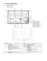
Page 6: ...ft SC Scan Drive A DC DC Converter Tuner Speaker out AV Terminal HDMI in SD Card Digital Signal Processor Nile TCON Format Converter Plasma AI Sub Field Processor Key Switch SS Sustain Drive SU Scan out Upper Non serviceable SU Board should be exchanged for service SD Scan out Lower Non serviceable SD Board should be exchanged for service K Remote receiver Power LED C A T S sensor S Power Switch 6...

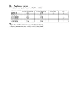
Page 7: ...480 60i 15 73 59 94 525 480 60p 31 47 59 94 750 720 60p 45 00 59 94 1 125 1 080 60i 33 75 59 94 1 125 1 080 60p 67 43 59 94 1 125 1 080 60p 67 50 60 00 1 125 1 080 24p 26 97 23 98 1 125 1 080 24p 27 00 24 00 Note Signals other than those shown above may not be displayed properly The above signals are reformatted for optimal viewing on your display 7 ...

Page 8: ...mm 786 432 1 024 W x 768 H 3 072 x 768 dots 20 W 10 W 10 W 10 THD VHF UHF 2 69 CATV 1 135 Temperature Humidity 32 F 104 F 0 C 40 C 20 80 RH non condensing RCA PIN Type x 1 1 0 V p p 75 Q RCA PIN Type x 2 0 5 V rms 1 0 V p p including synchronization 0 35 V p p RCA PIN Type x 2 0 5 V rms VIDEO AUDIO L R Y PB PR AUDIO L R TYPE A Connector x 2 This TV supports HDAVI Control 5 function SD CARD slot x ...

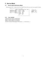
Page 9: ...J OPTION VSUS AGING SRV TOOL DTVSOC SOFT RB Cnt DTVSOC EEP LSI DATA STBY SOFT STBY EEP PDP SOFT до PDP EEP э с з с PDPFPGA PDPPDROM 3 3 fC EPOP I Sub Item 1 ADJUST i CONTRAST 0000 YMAX 5 1 1 Key command 1 button Main items Selection in forward direction 2 button Main items Selection in reverse direction 3 button Sub items Selection in forward direction 4 button Sub items Selection in reverse direc...

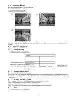
Page 10: ...ET EMERGENCY ON CLK MODE ON CLOCK FFF MIRROR 00 See next EDID CLK HIGH VSUS AGING ALL WHITE Built in test patterns can be AI ALL BLUE WHITE FLAME displayed AI ALL GREEN AI ALL RED LOW STEP WHITE LOW STEP BLUE LOW STEP GREEN LOW STEP RED RAMP WHITE RAMP RED RAMP GREEN RAMP BLUE A ZONE B ZONE 1 WINDOW COLOR BAR 9 POINT BRIGHTNESS WHITE FLAME AI ALL BLUE TWICE FIXATION 1 WINDOW SCROLL ON OFF OR RGBW ...

Page 11: ... PTCT 00 00 00 00 00 Time 00000 40 Count 01 POWER ON TIME COUNT Press MUTE button 3sec 5 3 2 Display of SOS History SOS History Number of LED blinking indication From left side Last SOS before Last three occurrence before 2nd occurrence after shipment 1st occurrence after shipment This indication except 2nd and 1st occurrence after shipment will be cleared by Self check indication and forced to fa...

Page 12: ...COMP2 VIDEO1 VIDEO2 OFF give priority to a last memory Channel Select channel when input signal is RF Set the channel each time power is switched on Selection Any channel number or means the channel when turns off Volume Adjust the volume when each time power is switched on Range 0 to 100 Vol Max Adjust maximum volume Range 0 to 100 OSD Ctrl Restrict the OSD Selection OFF PATTERN1 OFF No restricti...

Page 13: ...of units in hotel or any facility the data in master TV can be copied to SD card and then copy to other TVs 5 5 2 Preparation Make pwd file as startup file for a or b in a empty SD card 1 Insert a empty SD card to your PC 2 Right click a blank area in a SD card window point to New and then click text document A new file is created by default New Text Document txt 3 Right click the new text documen...

Page 14: ...wing password for a or b by using remote control a For Board replacement 2770 b For Hotel 4850 Data will be copied from TV set to SD card It takes around 2 to 6 minutes maximum for copying 4 After the completion of copying to SD card remove SD card from TV set 5 Turn off the TV set Note Following new folder will be created in SD card for data from TV set a For Board replacement user_setup b For Ho...

Page 15: ...SD card remove SD card from TV set a For Board replacement Data will be deleted after copying Limited one copy b For Hotel Data will not be deleted and can be used for other TVs 5 Turn off the TV set Note 1 Depending on the failure of boards function of Data copy for board replacement does not work 2 This function can be effective among the same model numbers e g For exchanging repair board Perfor...

Page 16: ...y shipment setting Produce TV reception screen and while pressing VOLUME button on the main unit press MENU button on the remote con trol for more than 3 seconds 6 1 2 Exit Disconnect the AC cord from wall outlet 6 1 3 Screen display 6 1 4 Check Point Confirm the following parts if NG was displayed DISPLAY Ref No Description P C B DTVSOC IC8001 Nile TCON A Board TUN TU8302 TUNER A Board MEM1 IC800...

Page 17: ...D Flashing timing chart 2 Contents When an abnormality has occurred the unit the protection circuit operates and reset to the stand by mode At this time the defective block can be identified by the number of blinks of the Power LED on the front panel of the unit 17 ...

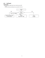
Page 18: ...6 3 No Power First check point There are following 2 states of No Power indication by power LED 1 No lit 2 Red is lit then turns red blinking a few seconds later See 6 2 No lit OK Check A board 18 ...

Page 19: ...6 4 No Picture Input only y v h a t s lnPut 0Г 1 У Signal 19 ...

Page 20: ...6 5 Local screen failure Plasma display may have local area failure on the screen Fig 1 is the possible defect P C B for each local area Fig 1 20 ...

Page 21: ... damaged if all connector is not removed for example remove connector only for SU board and stay connecting with SD board The board will be damaged 2 Connect SC jig to connector SC50 at left bottom side of SC board 3 Turn of the TV Display Unit and confirm the power LED blinking LED blinking Possible cause of failure is in SC board No LED blinking Lighting or no lighting Possible cause of failure ...

Page 22: ...e connector P9 3 Remove the screw x1 and remove the AC inlet 8 3 Remove the P Board Caution To remove PC B wait 1 minute after power was off for dis charge from electrolysis capacitors 1 Unlock the cable clampers to free the cable 2 Disconnect the connectors P2 P6 P7 P9 P11 and P35 3 Remove the screws x9 and remove the P Board 8 4 Remove the Side terminal cover and Side shield metal 1 Remove the s...

Page 23: ...he Speaker terminal 3 Remove the screws x2 each and remove the Speak ers L R 1 Remove the flexible cables SU1 SU2 SU3 and SU4 connected to the SU Board 2 Remove the flexible cable SU11 SD11 and the bridge connector SC41 SU41B 3 Remove the molding prop x1 O 4 Remove the screws x2 x2 сф and remove the SU Board 8 8 Remove the SU Board 8 9 Remove the SD Board 1 Remove the flexible cables SD1 SD2 SD3 a...

Page 24: ...ee the cable 3 Disconnect the connectors SS3 SS11 and SS23 4 Disconnect the flexible cables SS52 and SS55 5 Remove the screws x4 and remove the SS Board 8 12 Remove the Hanger metals and the Stand brackets 1 Remove the Plasma panel section from the servicing stand and lay on a flat surface such as a table covered by a soft cloth with the Plasma panel surface facing downward 2 Remove the Stand brac...

Page 25: ...8 5 2 Remove the Hanger metal L and the Stand bracket L See section 8 12 3 Remove the flexible cables holder fastening screws x8 O 4 Disconnect the flexible cables CB5 CB6 CB7 and CB8 5 Disconnect the flexible cables C20 and C21 6 Disconnect the connectors C23 and C25 7 Remove the screws x4 and remove the C2 Board 8 15 Remove the Plasma panel sec tion from the Cabinet assy glass 1 Remove the cabin...

Page 26: ...Open a box and without taking a new plasma panel Attach the C1 Board and the C2 Board connect the flexi ble cables from the plasma panel to the C1 Board and the C2 Board and fit the flexible cable holders 3 Attach the Hanger metals and the Stand brackets to the new plasma panel 4 Place the plasma panel on the servicing stand taking hold of the Hanger metals 5 Attach the cabinet assy and each P C B...

Page 27: ...y will be displayed during TEST and CONF stage Press 5 button to display the On Screen Display 3 Press VOL button to set to LOW 4 In LOW setting a If no several dead pixel is visible remarkably in white pattern press 3 button to go to CONF stage b If the several dead pixels are visible remarkably in white pattern Set to HIGH by press VOL button Press 3 button to go to CONF stage if the symptom is ...

Page 28: ...r bar The pattern for adjustment must contain 100 white part Procedure Remarks 1 Receive the sprit color bar with RF analog signal ASPECT FULL Picture menu Vivid 2 Enter Service mode menu and select ADJUST CONTRAST Pushing the remote controller OK key for about 3 seconds GAIN is suited to the adjustment value automatically 28 ...

Page 29: ...nd adjust B DRV and R DRV so x y value of color analyzer become the Color temperature High in table 2 8 Increase RGB together so the maximum drive value in RGB becomes FF That is set ALL DRIVE to FF Execute adjustment again When that the maximum value of R G B DRV should be FF and either R G B DRV should be FF Note Note In procedure 7 all description of data FF should be treated as data FC when th...

Page 30: ...7D 017E 017F 0180 0181 SD R CUTOFF 0182 Color temperatur G CUTOFF 0183 Mid B CUTOFF 0184 R DRIVE 0185 G DRIVE 0186 B DRIVE 0187 SD R CUTOFF 0188 Color temperatur G CUTOFF 0189 Low B CUTOFF 018A R DRIVE 018B G DRIVE 018C B DRIVE 018D HD R CUTOFF 018E Color temperatur G CUTOFF 018F High B CUTOFF 0190 R DRIVE 0191 G DRIVE 0192 B DRIVE 0193 HD R CUTOFF 0194 Color temperatur G CUTOFF 0195 Mid B CUTOFF ...

Page 31: ... CUTOFF 01 AC Color temperatur G CUTOFF 01 AD Low B CUTOFF 01AE DIFF R DRIVE 01AF G DRIVE 01 B0 B DRIVE 01 B1 HD R CUTOFF 01 B2 Color temperatur G CUTOFF 01 B3 High B CUTOFF 01 B4 DIFF R DRIVE 01 B5 G DRIVE 01 B6 B DRIVE 01 B7 HD R CUTOFF 01 B8 Color temperatur G CUTOFF 01 B9 Mid B CUTOFF 01 BA DIFF R DRIVE 01 BB G DRIVE 01 BC B DRIVE 01 BD HD R CUTOFF 01 BE Color temperatur G CUTOFF 01 BF Low B C...

Page 32: ...32 ...

Page 33: ...10 Block Diagram 10 1 Main Block Diagram A D IG ITAL SIG NAL PROCESSO R 33 ...

Page 34: ...10 2 Block 1 4 Diagram ...

Page 35: ...10 3 Block 2 4 Diagram A D IG ITAL SIG N AL PROCESSO R 35 ...

Page 36: ...10 4 Block 3 4 Diagram I p PO W ER SUPPLY 36 ...

Page 37: ...10 5 Block 4 4 Diagram s C s c a n d r iv e SS SU STAIN DRIVE PLASMA PANEL PANEL SUSIAIN ELECTRODE 37 ...

Page 38: ...38 ...

Page 39: ...gram 11 1 Caution statement Caution Please confirm that all flexible cables are assembled correctly Also make sure that they are locked in the connectors Verify by giving the flexible cables a very slight pull 11 2 Wiring 1 39 ...

Page 40: ...11 3 Wiring 2 40 ...

Page 41: ...11 4 Wiring 3 41 ...

Page 42: ...42 ...

Page 43: ...Chassis Earth Cold Line Earth Hot 6 Voltage Measurement Voltage is measured by a DC voltmeter Conditions of the measurement are the following Power S ource AC120V 60Hz Receiving S ignal Colour Bar signal RF All customer s controls Maximum positions 7 When arrow mark is found connection is easily found from the direction of arrow 8 Indicates the major signal flow Video A u d io s 9 This schematic d...

Page 44: ...old Precautions a Do not touch the hot part or the hot and cold parts at the same time or you may be shocked b Do not short circuit the hot and cold circuits or a fuse may blow and parts may break c Do not connect an instrument such as an oscilloscope to the hot and cold circuits simultaneously or a fuse may blow Connect the earth of instruments to the earth connection of the circuit being measure...

Page 45: ...D C IC8Q0 C 2 1 A V D D 3 3 A D A C I G P IO IR Q _24KE c TU TO 9 14 SD TO 3 14 T P 5 M1 TO 11 14 P A N El_test_ on vdd2 s_en Q Ц E E I Г tЦ i l l G pIE E Е о г l B ICKoJ F2 IR Q 1 PO SHERX R S T B e IC8 4 G 2 4 IR Q 2 R Q i E T H E RIR Q B B TO 8 14 arC 1 _ offО IC80310 AAi11IR Q 3 IR Q P O W E RD E T2 4 K E C H 1 I h E B G E S E R L S U B L t ш n iH G Z TO 6 14 audio_xrst O TO 12 14 pane l _ al ...

Page 46: ...A DDR2 800M z x 16bit Bp B E Щ 5 M 5 i a s B I B D D R C LK m5 D R B C L K A D 1 6 0 001 iHZEEl Сзшг та л1 2 l ic Q N 3 jД 4 l юзшгО L 7 c сгозгО к ю 0 и nc и з I ic 3 o o W 1 5 S T E 1сзоогО n T a 5 l icaojgQ Р 7 ли 4 с о U Ч с О м и С 3шгО ш 1 0 4 0 н Ь с ш ш О вл 1 H Q ю 11 12 13 ...

Page 47: ...14 15 16 17 18 45 ...

Page 48: ...12 4 А Board 3 14 Schematic Diagram A A B O A R D TXN A1 LNUUS 3 14 N O R S D card E EP TO 1 10 14 ж I IC8502 TVRR693AGS 128Mbit NOR FLASH Ц Г 19 20 21 22 23 46 ...

Page 49: ...24 25 26 27 ...

Page 50: ...12 5 А Board 4 14 Schematic Diagram A A B O A R D TXN A1 LNUUS 4 14 P O W E R SU P P LY 28 29 30 31 32 47 ...

Page 51: ...I j SUB3 3V T T 1 _ l Iц s T г 1 IC5605 C0DBAGF00030 SUB3 3V C0DBGYY00887 SUB3 3V_A SUB3 3VJHDMI C0DBGYY00887 SUB3 3V_HDMI SUB3 3V_SD T T I IC5613 CODBGYY00893 SUB3 3V SD I 33 34 35 ...

Page 52: ...12 6 А Board 5 14 Schematic Diagram A A B O A R D TXN A1 LNUUS 5 14 A V S W PC M O D EL TO 1 14 r 37 38 39 40 ...

Page 53: ...TU TO 9 14 PD P U S YPBPR 1 114 l r S r r К I i t J 5 J i l b L T i 1 4 US A V 2 T R 2 2 S 0 TO 7 14 J i 1 Г TO 1 14 cr j u i r iM 41 42 43 44 48 ...

Page 54: ...12 7 A Board 6 14 Schematic Diagram A A B O A R D TXN A 1LN U U S 6 14 A U D IO AM P TO SPEAKER 46 47 48 49 50 51 52 53 54 49 ...

Page 55: ...ematic Diagram A A B O A R D TXN A 1LN U U S 7 14 A V TE R M IN A L A N A LO G ASIC A V TER M IN AL JK2103 K2HA918A0002 AV TERMINAL TO 5 14 S ID E T ER M IN AL JK2111 K4AK08B00005 SIDE TERMINAL 55 56 57 58 59 60 61 62 63 50 ...

Page 56: ...12 9 A Board 8 14 Schematic Diagram A A B O A R D TXN A 1LN U U S 8 14 HDMI 64 65 66 67 68 69 70 71 72 51 ...

Page 57: ...12 10 A Board 9 14 Schematic Diagram 52 ...

Page 58: ...12 11 A Board 10 14 K Board and S Board Schematic Diagram A A B O A R D TX N A 1LN U U S 10 14 C O N N E C TO R 82 83 84 85 86 87 88 89 90 53 ...

Page 59: ...12 12 A Board 11 14 Schematic Diagram A 91 92 93 94 95 96 97 98 99 TO 1 6 10 14 54 0 0 0 ...

Page 60: ...12 13 A Board 12 14 Schematic Diagram 100 1 101 1 102 1 103 1 104 1 105 1 106 1 107 1 108 55 ...

Page 61: ... D D 2 P D P C j3 _ P D P C j4 _ P D C tR R 9 4 7 N O D D E D E X B P D p c j2 _ lP D C L R D 1 ___ 3 4 J V D O D E D 1 D P C D 2 r a r e M I Ш1 н n il и ж ii ш t r o f f E r ЕШ 9999 n i I n S 3 jj J S j i S i S 1 3 I SS i 1 3 i i cfj S Jj гii1 109 110 111 112 113 114 115 116 117 IO A33 C1 BOARD C11 56 ...

Page 62: ...12 15 A Board 14 14 Schematic Diagram Ш 222 TO A34 C2 BOARD C21 118 119 120 121 122 123 124 126 126 57 ...

Page 63: ...12 16 C1 Board Schematic Diagram D A C1 B O A R D T X N C 11LNUU 58 ...

Page 64: ...1 I Н X I I H I I I 6 7 8 9 ...

Page 65: ...12 17 C2 Board Schematic Diagram A C D B E F i 2 3 4 8 9 5 59 ...

Page 66: ...12 18 SC Board 1 4 Schematic Diagram A C D A S C BO AR D TX N S C 1LN U U 1 4 TO B E F 1 2 3 4 6 8 9 5 7 60 ...

Page 67: ...12 19 SC Board 2 4 Schematic Diagram 10 11 12 13 14 15 16 17 18 61 ...

Page 68: ...12 20 SC Board 3 4 Schematic Diagram A S C BO AR D TXN S C 1LN U U 3 4 19 20 21 22 23 24 25 26 27 62 ...

Page 69: ...12 21 SC Board 4 4 Schematic Diagram A S C BO AR D TXN S C 1LN U U 4 4 28 29 30 31 32 33 34 35 36 63 ...

Page 70: ...12 22 SS Board 1 2 Schematic Diagram A C D A B E F 6 5 7 64 ...

Page 71: ...12 23 SS Board 2 2 Schematic Diagram A SS BO A R D TX N S S1LN U U 2 2 PANEL SUSTAIN ELECTRODE PANEL SUSTAIN ELECTRODE 10 11 12 13 14 15 16 17 18 65 ...

Page 72: ...13 Printed Circuit Board 13 1 К and S Board 6 5 K BOARD FOIL SIDE TXN K1LFUUM CRNO 2E0D TNPA5125 S E E R E V E R S E FOR O R D E R NO K BOARD COMPONENT SIDE TXN K1LFUUM 1 A I В I С I D ...

Page 73: ...S BOARD FOIL SIDE TXN S1EQUUM S BOARD COMPONENT SIDE TXN S1EQUUM F I G I H ...

Page 74: ...Z9 9 SnnNI l V NXl aais nod aavoa v pjeog v Z ZV ...

Page 75: ...68 ...

Page 76: ...13 3 C1 Board C1 BOARD FOIL SIDE TXNC11LNUU C1 BOARD COMPONENT SIDE TXNC11LNUU IIP i шшш TN P A 5 0 7 9 I G 6 5 4 3 2 1 E F H 69 ...

Page 77: ...13 4 C2 Board 6 3 C2 BOARD COMPONENT SIDE TXNC21LNUU 70 ...

Page 78: ...13 5 SC Board 71 ...

Page 79: ...SC BOARD COMPONENT SIDE TXNSC1LNUU G 6 5 4 3 2 1 E F H 72 ...

Page 80: ...13 6 SS Board 6 5 4 SS BOARD FOIL SIDE TXNSS1LNUU ...

Page 81: ...1 I F I G I H 73 ...

Page 82: ...6 5 4 SS BOARD COMPONENT SIDE TXNSS1LNUU A В С D ...

Page 83: ...74 ...

Page 84: ...14 Exploded View and Replacement Parts List 14 1 Exploded View and Mechanical Replacement Parts List 14 1 1 Exploded View 1 75 ...

Page 85: ...14 1 2 Exploded View 2 76 ...

Page 86: ...14 1 3 Accessories 77 ...

Page 87: ...14 1 4 Mechanical Replacement Parts List Note All parts except parts mentioned PAVCA in the Remarks column are supplied byAVC CSPC Parts mentioned PAVCA are supplied by PAVCA 78 ...

Page 88: ... 16 C 8 24 11 TKGA5 610 FRONT GLASS 1 PAVCA 12 TKK2AA9402 LED PANEL 1 PAVCA 13 TKKL5 493 M8 CAP 4 14 TMK2AG08005 SPONGE FRONT GLASS UPPER BOTTOM 2 PAVCA 15 TMK2AG0800 6 SPONGE FRONT GLASS LEFT RIGHT 2 PAVCA TMM2 3417 CLAMPER 2 TMME3 31 CLAMPER P 1 1 TMME332 CLAMPER HANGER 4 4 TMME332 CLAMPER SS 1 1 TMME332 CLAMPER 2 TMME332 CLAMPER 2 TMME3 41 CLAMPER 2 16 TMW2AA0 03 SP BRACKET L 2 PAVCA 17 TMW2AA0...

Page 89: ...LQUU SPEAKER LEAD A11 SPR SPL 1 PAVCA XSB3 6FJ SCREW HDMI 3 2 XTB4 12GFJ SCREW GH 20 PW 2 LED 1 23 XTB4 12GFJK SCREW BC 11 11 XTB4 12GFN SCREW 4 12 6 XTV3 10JFJK SCREW REAR AV 2 2 XTW3 10TFJ SCREW 1 XYN3 F10FJK SCREW BC AC INLET 2 2 XYN3 J10FJ SCREW 17 XYN4 E6FJ SCREW INLET 1 1 XYN4 F10FJ SCREW 6 XYN4 F10FJ SCREW SUSD 4 4 XYN4 F10FJ SCREW HANGER METAL ASSY 4 4 XYN4 F10FJ SCREW SP BRKT 4 4 XYN4 F10...

Page 90: ...pe of assembly and in accordance with the laws governing part and product retention After the end of this period the assembly will no longer be available Abbreviation of part name and description 1 Resistor 2 Capacitor Example Example ERD25TJ104 С ЮОКОНМ J 1 4W ECKF1H103ZF С 0 01UF Z 50V Type Allowance Type Allowance Type Allowance С Carbon F 1 F Fuse G 2 M Metal Oxide J 5 Metal Film К 10 S Solid ...

Page 91: ...C 1000UF 50V 1 C4733 F1G1H102A7 30 C 1000UF 50V 1 C4734 F1G1H102A7 30 C 1000UF 50V 1 C4735 F1G1H102A7 30 C 1000UF 50V 1 C4740 F1G1C104A116 C 0 10UF K 16V 1 C4741 F1G1C104A116 C 0 10UF K 16V 1 C4744 F1G1H102A7 30 C 1000UF 50V 1 C4745 F1G1C104A116 C 0 10UF K 16V 1 C4746 F1G1H102A7 30 C 1000UF 50V 1 C4747 F1G1C104A116 C 0 10UF K 16V 1 Safety Ref No Part No Part Name Description Pcs Remarks A PCB TXN ...

Page 92: ...07 E 47UF 25V 1 C5734 F1J1E105A231 C 1 UF 25V 1 C5736 F1G1A105A047 C 1UF K 10V 1 Safety Ref No Part No Part Name Description Pcs Remarks C5737 F1G1A105A047 C 1UF K 10V 1 C5738 F1G1A105A047 C 1UF K 10V 1 C5739 F1G1A105A047 C 1UF K 10V 1 C5764 ECJ1VB1A105K C 0 01UF Z 50V 1 C5765 ECJ1VB1A105K C 0 01UF Z 50V 1 C5771 F1H1E333A129 C 0 033UF 25V 1 C5776 ECJ1VB1A105K C 0 01UF Z 50V 1 C5777 ECJ1VB1A105K C ...

Page 93: ...390A731 C 39UF 50V 1 C8337 F1G1H121A731 C 120PF K 50V 1 C8338 F1G1H121A731 C 120PF K 50V 1 C8339 F1G1H680A731 C 68UF 50V 1 C8342 F1G1C104A116 C 0 10UF K 16V 1 C8343 F1G1C104A116 C 0 10UF K 16V 1 Safety Ref No Part No Part Name Description Pcs Remarks C8349 F1G1H102A730 C 1000UF 50V 1 C8350 F1G1C104A116 C 0 10UF K 16V 1 C8351 F1G1H102A730 C 1000UF 50V 1 C8352 F1G1C104A116 C 0 10UF K 16V 1 C8353 F1J...

Page 94: ...ety Ref No Part No Part Name Description Pcs Remarks C16192 F1H1E104A129 C 0 1UF 25V 1 C16193 EEUFC1E470 E 47UF 25V 1 C16195 F1K1E105A029 C 1UF Z 25V 1 C16242 F1H1C105A145 C 0 01UF K 16V 1 C16243 F1H1H103A970 C 0 001UF K 50V 1 C16244 F1J1A106A087 C 0 010UF K 10V 1 C16272 F2A1E471A102 E 470UF 25V 1 C16286 F1H1H104A970 C 0 1UF K 50V 1 C16287 F1H1H104A970 C 0 1UF K 50V 1 C16310 F2A2T251A004 E 250UF 2...

Page 95: ...ME000076 DIODE 1 D4704 B0ACCJ000048 DIODE 1 D5603 B0ACCJ000048 DIODE 1 D5604 B0ACCJ000048 DIODE 1 D5605 B0ACCJ000048 DIODE 1 D5606 B0JCCE000008 DIODE 1 D5629 B0BC8R200004 DIODE 1 PAVCA D5633 B0ACCJ000048 DIODE 1 D5670 B0JCCE000008 DIODE 1 Safety Ref No Part No Part Name Description Pcs Remarks D5671 B0JCCE000008 DIODE 1 D5765 B0HCMM000014 DIODE 1 D5770 B0JCPG000030 DIODE 1 D5771 B0JCPG000030 DIODE...

Page 96: ...PAVCA JK2111 K4AK08B00005 TERMINAL 1 PAVCA JK4500 K1FY119D0013 CONNECTOR 1 PAVCA JK4501 K1FY119D0013 CONNECTOR 1 PAVCA JK8502 K1NA09E00080 9P CONNECTOR 1 JS3700 D0GBR00Z0002 M 0 OHM J 1 10W 1 JS3701 D0GBR00Z0002 M 0 OHM J 1 10W 1 JS4017 D0GBR00Z0002 M 0 OHM J 1 10W 1 JS4018 D0GBR00Z0002 M 0 OHM J 1 10W 1 JS4022 D0GBR00Z0002 M 0 OHM J 1 10W 1 JS4700 ERJ6GEY0R00V M 0 OHM J 1 10W 1 JS4701 ERJ6GEY0R00...

Page 97: ... 1 Q16161 B1HFPFA00001 TRANSISTOR 1 Q16191 B1HFPFA00001 TRANSISTOR 1 Q16280 B1ABCF000231 TRANSISTOR 1 Q16401 B1JAEQ000010 TRANSISTOR 1 PAVCA Safety Ref No Part No Part Name Description Pcs Remarks Q16402 B1JAEQ000010 TRANSISTOR 1 PAVCA Q16421 B1JAEP000014 TRANSISTOR 1 PAVCA Q16422 B1JAEP000014 TRANSISTOR 1 PAVCA Q16441 DG3D5010CSLW ZENER DIODE 1 PAVCA Q16451 B1JAEP000012 TRANSISTOR 1 Q16471 B1ABCF...

Page 98: ... OHM J 0 063W 1 R4507 ERJ2GEJ103 M 10KOHM J 0 063W 1 R4512 D0GA473JA015 M 47 OHM J 0 063W 1 Safety Ref No Part No Part Name Description Pcs Remarks R4516 D0GA473JA015 M 47 OHM J 0 063W 1 R4519 ERJ2GEJ102X M 1K OHM J 1 4W 1 R4520 ERJ2GEJ102X M 1K OHM J 1 4W 1 R4525 D0GA472JA015 M 4 7KOHM J 0 063W 1 R4526 D0GA472JA015 M 4 7KOHM J 0 063W 1 R4548 ERJ2GEJ220 M 22 OHM J 0 063W 1 R4549 D0GA151JA015 M 150...

Page 99: ...XB28V101JX RESISTOR ARRAY 1 R8013 EXB28V101JX RESISTOR ARRAY 1 R8014 EXB28V101JX RESISTOR ARRAY 1 R8015 EXB28V101JX RESISTOR ARRAY 1 R8016 EXB28V101JX RESISTOR ARRAY 1 R8017 EXB28V101JX RESISTOR ARRAY 1 R8018 EXB28V101JX RESISTOR ARRAY 1 R8019 EXB28V101JX RESISTOR ARRAY 1 R8023 D0GA105JA015 M 1M OHM J 0 063W 1 R8024 D0GA152JA015 M 1 5KOHM J 0 063W 1 Safety Ref No Part No Part Name Description Pcs ...

Page 100: ...W 1 R9023 D0GA272JA015 M 2 7KOHM J 0 063W 1 R9026 D0GAR00Z0001 C 0 OHM 0 063W 1 R9027 D0GAR00Z0001 C 0 OHM 0 063W 1 Safety Ref No Part No Part Name Description Pcs Remarks R9028 D0GA101JA015 M 100 OHM J 0 063W 1 R9029 D0GA101JA015 M 100 OHM J 0 063W 1 R9030 D0GAR00Z0001 C 0 OHM 0 063W 1 R9070 ERJ2GEJ103 M 10KOHM J 0 063W 1 R9072 ERJ2GEJ103 M 10KOHM J 0 063W 1 R9100 D0GA473JA015 M 47 OHM J 0 063W 1...

Page 101: ... R9984 D0GA472JA015 M 4 7KOHM J 0 063W 1 R9985 D0GA472JA015 M 4 7KOHM J 0 063W 1 Safety Ref No Part No Part Name Description Pcs Remarks R9986 D0GA472JA015 M 4 7KOHM J 0 063W 1 R9998 D1BA1601A014 M1 60KOHM 1 10W 1 PAVCA R9999 D0GAR00Z0001 C 0 OHM 0 063W 1 R16001 ERJT08J7R5V M 7 5OHM J 0 33W 1 R16002 ERJT08J7R5V M 7 5OHM J 0 33W 1 R16021 ERJT08J7R5V M 7 5OHM J 0 33W 1 R16022 ERJT08J7R5V M 7 5OHM J ...

Page 102: ...84 D1BD6811A044 M6 81KOHM 1 10W 1 R16585 D1BB1001A055 M 1KOHM 1 16W 1 R16586 D1BB1691A055 M1 69KOHM 1 10W 1 PAVCA R16587 D0GB222JA041 M 2 2KOHM J 1 10W 1 Safety Ref No Part No Part Name Description Pcs Remarks R16588 D0GB103JA057 M 10K OHM J 1 10W 1 R16590 ERJ3GEYJ221 M 220 OHM J 1 16W 1 R16591 EXB38V472JV RESISTOR ARRAY 1 R16593 D1BB1331A055 M1 33KOHM 1 10W 1 PAVCA R16601 ERJT08J1R0V M 1 8OHM J 0...

Page 103: ...A057 M 10K OHM J 1 10W 1 R16926 D0GB222JA041 M 2 2KOHM J 1 10W 1 R16927 ERJ6GEYJ223 M 22KOHM J 1 10W 1 R16928 ERJ6GEYJ4 72V M 4 7K OHM J 1 10W 1 Safety Ref No Part No Part Name Description Pcs Remarks R16929 ERJT08J1R0V M 1 8OHM J 0 33W 1 R16930 D1BF2R70A021 M 2 7 OHM 1 10W 1 R16931 D1BF2R70A021 M 2 7 OHM 1 10W 1 R16932 ERJ6GEYJ223 M 22KOHM J 1 10W 1 R16933 D1BB1002A055 M 10KOHM 1 10W 1 R16934 D1B...

Page 104: ...Y03B00006 3P CONNECTOR 1 SS23 K1KY06AA0719 6P CONNECTOR 1 SS52 K1MY13BA0376 13P CONNECTOR 1 PAVCA SS55 K1MY13BA0376 13P CONNECTOR 1 PAVCA SW2500 K0F122A00172 SWITCREMOTE CON TROLH 1 SW3759A K0H1BA000445 SWITCH 1 SW3761A K0H1BA000445 SWITCH 1 SW3762A K0H1BA000445 SWITCH 1 SW3763A K0H1BA000445 SWITCH 1 SW3764A K0H1BA000445 SWITCH 1 SW3765A K0H1BA000445 SWITCH 1 T16471 G4DYA0000201 TRANSFORMER 1 PAVC...

Reviews: