Pin
No.
Mark
I/O /
Division
Function
1
PGND1
—
Connected to GND
2
DSW
O
DC/DC converter coil drive
terminal
3
PVCC1
I
Power supply input terminal
4
VSEN
I
Empty detection input
terminal (Connected to
power supply)
5
RESTART
I
DC/DC converter drive input
terminal (Connected to
power supply through
capacitor)
6
ICNT
I
Setting of charging current
input terminal (Connected to
GND through resistor)
7
AMUTE
O
Muting signal output
terminal
8
START
I
Starting of DC/DC converter
input terminal
9
VG
I
Power supply input terminal
10
LG
I
Coil drive input terminal for
VG voltage increase /
(connected to power supply)
11
PGND2
—
Connected to GND
12
IOUT
O
Charging signal and
charging feedback output
terminal
13
PVCC2
I
Power supply input terminal
14
PEGB
O
Regulator drive signal
output terminal
15
MSTAT/
/
ACDET
O
DC jack detection output
terminal
16 MDATA/
/ EMP
I
Power drop detection input
terminal
17
MLD/ /
VCNT
I
Regulator voltage switching
input terminal
18
MCLK/
/
CHARGE
I
Charging ON/OFF input
terminal
19
S/P
I
Serial/parallel switching
input terminal (Connected to
power supply)
20
DVDD
I
Power supply input terminal
28
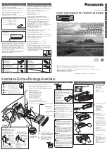
Summary of Contents for SLCT570 - PORT. CD PLAYER
Page 7: ...5 Operation Checks and Component Replacement Procedures 7 ...
Page 8: ...8 ...
Page 9: ...9 ...
Page 10: ...10 ...
Page 11: ...11 ...
Page 37: ...P1 RPK1332 PACKING CASE S 1 S GH 37 ...
Page 41: ...17 Packaging 41 ...