- Ground the soldering iron.
- Put a conductive mat on the work table.
- Do not touch the pins of IC or LSI with fingers directly.
11. Schematic Diagram
12. Printed Circuit Board and Wiring Connection
Diagram
13. Block Diagram
14. Terminal Function of IC's
14.1. IC101(AN8839NSBE1): Servo Amplifier
Pin
No.
Mark
I/O /
Division
Function
1
PDE
I
Tracking signal input (1)
terminal
2
I
Tracking signal input (2)
terminal
3
VDD
I
Power supply input terminal
4
PDA
I
Focus signal input (1)
terminal
5
PDB
I
Focus signal input (2)
terminal
6
LPD
I
APC amplifier input terminal
7
LD
O
APC amplifier output
terminal
8
RF
O
RF addition output terminal
9
RF IN
I
RF detection signal input
terminal
10
CSBRT
I
Capacitor connection
terminal for OFTR
11
CEA
I
HPF amplifier capacitor
connection input terminal
12
BDO
O
Dropout signal output
terminal
(H: dropout)
13
LDON
I
APC control input terminal
14
GND
—
Connected to GND
15
/RFDET
O
RF detection signal output
terminal / (L: detection)
20
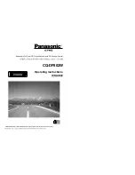
Summary of Contents for SLCT570 - PORT. CD PLAYER
Page 7: ...5 Operation Checks and Component Replacement Procedures 7 ...
Page 8: ...8 ...
Page 9: ...9 ...
Page 10: ...10 ...
Page 11: ...11 ...
Page 37: ...P1 RPK1332 PACKING CASE S 1 S GH 37 ...
Page 41: ...17 Packaging 41 ...