background image

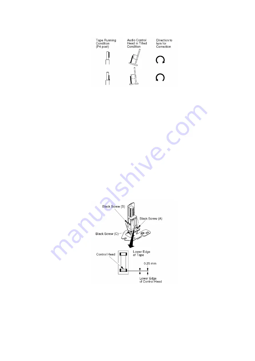
6.2.2.2.3. AUDIO CONTROL HEAD HEIGHT ADJUSTMENT
The height of the Audio Control Head replacement part is preset at the factory.

Purpose:

To be sure the tape runs properly along the Control Head.

Symptom of Misadjustment:

If the control signal is not properly picked up, Servo Operation 
cannot be achieved. A Blue screen will be seen in Playback.

This confirmation is required when the Audio Control Head is replaced.

1. Play back a T120 cassette tape and check that the lower edge of 

the tape runs approximately 0.25 mm above the lower edge of the 
Audio Control Head.

2. If necessary, adjust Black Screws (A) and (B) clockwise to lower 

the tape or counterclockwise to raise.

Fig. M6

6.2.2.2.4. AUDIO CONTROL HEAD AZIMUTH ADJUSTMENT

Purpose:

To adjust the position and height of the Audio Control Head so 
that it meets the tape tracks properly.

50

Summary of Contents for Omnivision PV-V4600

Page 1: ...ORDER NO MKE0001002C1 B3 Video Cassette Recorder PV V4600 PV V4620 PV V4620 K PV V4630 K PV V4640 PV V4640 K PV V4660 SPECIFICATIONS 1 SAFETY PRECAUTIONS GENERAL GUIDELINES 1 ...

Page 2: ...serve the original lead dress If a short circuit is found replace all parts which have been overheated or damaged by the short circuit 4 After servicing see to it that all the protective devices such as insulation barriers insulation papers shields are properly installed 5 After servicing make the following leakage current checks to prevent the customer from being exposed to shock hazards LEAKAGE ...

Page 3: ...zard and the equipment should be repaired and rechecked before it is returned to the customer Figure 1 2 PREVENTION OF ELECTRO STATIC DISCHARGE ESD TO ELECTROSTATICALLY SENSITIVE ES DEVICES Some semiconductor solid state devices can be damaged easily by static electricity Such components commonly are called Electrostatically Sensitive ES Devices Examples of typical ES devices are integrated circui...

Page 4: ...ted together byconductive foam aluminum foil or comparable conductive material 7 Immediately before removing the protective material from the leads of a replacement ES device touch the protective material to the chassis or circuit assembly into which the device will be installed CAUTION Be sure no power is applied to the chassis or circuit and observe all other safety precautions 8 Minimize bodily...

Page 5: ...ll be displayed in F I P The Simplified Fault finding data is stored in the Memory IC IC6005 This data is cleared after it is displayed and then the POWER button is pressed back on 1 With power turned off press VCR TV button on VCR for over 3 seconds if VCR is not in shut off condition Fig 1 1 2 Fault code 4 digit number will be displayed in F I P as shown Fig 1 2 Fig 1 3 Fig 1 4 5 ...

Page 6: ... on VCR with power turned off press any operation button on either VCR or remote to detect that a key has been pressed The 1st digit changes to 0 only when key is detected Fig 1 7 4 When 1 to 4 listed in Lock code occurs Lock data will be stored 6 ...

Page 7: ...isplays the Total lapsed time with power on day and the Total lapsed time with Cylinder rotation hour on the TV monitor 1 With power turned on without a cassette press VCR TV button on VCR and 7 key on remote together The USAGE SCREEN will be displayed on the TV Monitor Fig 1 9 Note After replacing the Cylinder Unit press COUNTER RESET button on remote in this mode Only Total lapsed time with Cyli...

Page 8: ...STMENT in ELECTRICAL ADJUSTMENT procedures 4 1 4 SERVICE POSITION 4 1 4 1 Service Position CAUTION HOT CIRCUIT Primary circuit exists on the Main C B A Use extreme care to prevent accidental shock when servicing 4 1 4 1 1 Service Position 1 Fig 2 1 4 1 4 1 2 Service Position 2 Fig 2 2 8 ...

Page 9: ... for the Frame as shown in Fig 2 2 2 When recording in Service Position 2 short the S Tab SW Pins on foil side of Main C B A to turn this SW on Fig 2 3 3 Place the tape between the Cassette Up Ass y and Main C B A to get a stability 4 When disassembling assembling refer to CABINET SECTION in 9 ...

Page 10: ...ds in power off condition Fig 3 1 The power comes on and the unit goes into service mode In this mode Mechanism movement can be confirmed When removing Cassette Up Ass y it can be confirmed without a cassette To release from this mode press POWER button off or disconnect AC Plug 4 1 7 TRACKING CENTER MODE TRACKING FIX AT CENTER Insert the Cassette tape Set the unit into Service Mode Play back the ...

Page 11: ...stall the Front Panel Ass y as follows 1 Swing the Cassette Door Lid all the way open until the Cassette Door tab clears the Opener Lever 2 Make sure that all locking tabs are aligned properly Then press the Front Panel straight in Fig 4 4 1 9 METHOD FOR LOADING UNLOADING OF MECHANISM Manual Method Turn the Loading Gear clockwise for loading or counterclockwise for unloading using needlenose plier...

Page 12: ...on a DC to Portion b CAUTION Before applying DC Power Supply be sure to disconnect the Motor Leads from the Connector P2503 Otherwise the Loading Motor Drive IC IC2501 may be damaged Fig 5 2 When loading without a cassette push Portion a on the Holder Unit of Cassette Up Ass y so that the Lever clear the First Tab and Second Tab Fig 5 3 12 ...

Page 13: ...move a jammed tape as follows 4 1 10 1 Manual Method When a tape jam is encountered check the tape loading condition and use the following procedure to remove a tape jam Fig 6 1 4 1 10 1 1 Method 1 1 Move the Pinch Roller Unit out by unhooking the Pin of Pinch Arm Unit so that the Pinch Roller is separated from the Capstan Rotor Unit shaft Fig 6 2 13 ...

Page 14: ...e pulling the Cassette Up Ass y out far enough so that it clears the Drive Rack Arm slide the Drive Rack Unit as indicated by the arrow to remove the cassettetape from the Cassette Up Ass y 7 Check the cause of mechanical trouble and repair Fig 6 3 4 1 10 1 2 Method 2 1 Rotate Loading Motor counterclockwise with needlenose pliers etc so that the Pinch Roller is separated from the shaft of the Caps...

Page 15: ...by rotating the Loading Gear CAUTION 1 Before applying DC Power Supply be sure to disconnect the Motor Leads from the Connector P2503 Otherwise the Loading Motor Drive IC IC2501 may be damaged 2 If loading does not start in approx 2 seconds after DC Power Supply is applied DO NOT continue to apply DC Power Supply Instead perform Manual Method 1 Be sure to disconnect the Motor Leads from the Connec...

Page 16: ...e Use a transformer of adequate power rating as this protects the technician from accidents resultingin personal injury from electrical shocks It will also protect VCR from being damaged by accidental shorting that may occur during servicing Also when troubleshooting the above type of Power Supply Circuit a variable isolation transformer is required in order to increase the input voltage slowly 4 ...

Page 17: ...ctrodes is melted remove the leadless component with a twisting motion Note A Do not attempt to lift the component off the board until the component is completely disconnected from the board by a twisting action B Be careful not to break the copper foil on the printed circuit board Fig 8 1 3 Installing the leadless component A Presolder the contact points on the circuit board Fig 8 2 B Press the p...

Page 18: ...NTIFICATION MARK Use Marks shown in the chart below to distinguish the different models included in this Service Manual 4 2 IC TRANSISTOR AND CHIP PART INFORMATION 4 2 1 HOW TO READ THE IDENTIFICATION MARK OF CHIP COMPONENTS 18 ...

Page 19: ...APACITOR Because of the width of the color bands the reading direction cannot be specified However the color band can be read on either side Be sure to confirm the value using the schematic diagram CAUTION Once chip parts are removed they must not be reused Always use a new part when installing a chip part 5 DISASSEMBLY ASSEMBLY PROCEDURES 5 1 CABINET SECTION 5 1 1 Disassembly Flowchart Perform al...

Page 20: ... numbers are also used as the identification location No of parts in Figures B Part to be removed or installed C Fig No showing Procedure or Part Location D Identification of part to be removed unhooked unlocked released unplugged or unsoldered 2 S 1 2 Screws S 1 2 L 1 2 Locking Tabs L 1 P 1 Spring P 1 E Refer to Notes in chart Fig D2 20 ...

Page 21: ... the tab on the Front Panel Ass y fits into the hole in the Top Cover Then lower the rear portion into place and tighten 2 Screws S 1 and 2 Screws S 2 2 Installation of Front Panel Ass y CAUTION Opener Lever may be damaged when Front Panel Ass y is installed with Cassette Door Lid of Front Panel Ass y and Opener 21 ...

Page 22: ... UNLOADING OF MECHANISM in SERVICE NOTES totighten screws Then slide it back to the EJECTPosition Make sure that Mechanism and Cassette Up Ass y are in the EJECT Position Refer to EJECT Position Confirmation in DISASSEMBLY ASSEMBLYPROCEDURES 4 Installation of Mechanism Chassis and Cassette Up Ass y onto Main C B A A Make sure the Mode Select SW on the Main C B A is in EJECT position If not rotate ...

Page 23: ...firm that the Locking Tab L 7 under the Cassette Up Ass y is in Hole on the Mechanism Chassis when installing the Cassette Up Ass y Then slide the Cassette UpAss y towards the back B When installing 2 Screws S 9 slide the Holder Unit Refer to METHOD FOR LOADING UNLOADING OF MECHANISM in SERVICE NOTES to tighten screws Then slide it back to the EJECTPosition C Hook Spring P 1 to the Drive Rack Arm ...

Page 24: ...5 2 2 Inner Parts Location Fig J1 1 24 ...

Page 25: ...5 2 3 EJECT Position Confirmation Fig J1 2 25 ...

Page 26: ...5 2 4 Grounding Plate Unit Full Erase Head and Cylinder Unit Fig J2 1 26 ...

Page 27: ...is positioned on the front side of the Cylinder shaft so that the center line of the plateis just less than 1 0 mm measured from the center of the Cylinder shaft If required adjust the plate position by loosening Screw S 1 Never install the Grounding Plate Unit on the rear side of the Cylinder shaft Incorrect positioning will cause cylinder buzz Fig J2 2 27 ...

Page 28: ...lacing the Cylinder Unit clear the Total lapsed time with Cylinder rotation hour to 0 Refer to USAGE SCREEN MODE in SERVICE NOTES 5 2 5 Capstan Belt Support Angle Intermediate Gear B and Main Cam Gear Fig J3 1 28 ...

Page 29: ... Rod A Confirm that the hole on Main Rod is a Through Hole with a hole on chassis B Confirm that the hole on Drive Rack Arm is a Through Hole with a hole on chassis C Install the Main Cam Gear so that the projection of Main Cam Gear is in the upward position as shown Fig J3 2 29 ...

Page 30: ...ole with a hole on chassis B Confirm that the hole on Intermediate Gear A is aligned with the hole on Lift Gear Fig J3 3 C Install the Intermediate Gear B so that the hole on the Intermediate Gear B is aligned with the hole on the Main Cam Gear Fig J3 4 3 Holes on Main Cam Gear A The EJECT mode Hole on Main Cam Gear should be a Through 30 ...

Page 31: ...acement part 5 Installation of Main Cam Gear and Main Cam Push Nut A After installing the Support Angle install the Main Cam Push Nut with Needlenose Pliers etc so that it is flush with the chassis There may be some slight scratches on the Shaft of Main Cam Gear when removing the Main Cam Gear In case that the Main Cam Gear can be installed securely without tottering it is fine to use the one If a...

Page 32: ...Fig J4 1 5 2 6 1 Reassembly Notes 1 Installation of Center Clutch Unit A Fit the Center Clutch Unit into the Changing Gear Fig J4 2 5 2 7 Reel Gear Main Rod and SS Brake Arm Unit Model E F G Fig J5 1 32 ...

Page 33: ...Unit A Align the Gear of T Loading Arm Unit with Gear of Main Rod Confirm that the Hole on Main Rod is a Through Hole with a hole on chassis Fig J5 2 5 2 8 Stopper Angle Capstan Rotor Unit Oil Seal Capstan Stator C B A MR Head and Sub Rotor Unit Model E F G Fig J6 1 33 ...

Page 34: ...f Silicon Grease CAUTION When installing the IC2501 AN3845SC or AN3846SC or Capstan Stator C B A be sure to apply Silicon Grease VFK1301 as shown Be careful not to touch other parts with greased portion to prevent grease depletion Fig J6 2 34 ...

Page 35: ...tan Rotor Unit Shaft into the hole of the Capstan Holder Unit so that shaft passes through 2 Oil Seals Be carefulnot to scratch the Shaft or Capstan Holder Unit B Align the bottom of Oil Seal A with notch line A Align the top of Oil Seal B with notch line B Fig J6 3 5 2 9 T Loading Arm Unit and S Loading Arm Unit Fig J7 1 35 ...

Page 36: ...ssis B Install the T Loading Arm Unit so that the hole on T Loading Arm Unit is aligned with the hole on S Loading Arm Unit C Confirm that the holes on the S T Loading Arm Unit are Through Holes with hole on chassis Fig J7 2 5 2 10 T Brake Unit Tension Control Arm Unit T Reel Table S Reel Table and Tension Arm Unit Fig J8 1 36 ...

Page 37: ...ssist Spring or the Tension Arm Unit replace only the Tension Arm Unit with a new one and remove the Assist Spring 5 2 10 1 Reassembly Notes 1 How to distinguish between S Reel Table and T Reel Table Fig J8 2 5 2 11 Loading Post Base T Unit and Loading Post Base S Unit Fig J9 37 ...

Page 38: ...gnment of Intermediate Gear A Lift Gear and P5 Arm Unit A Rotate the Lift Gear so that Hole A on Lift Gear is a Through Hole with a hole on chassis B Install the Intermediate Gear A so that the hole on Intermediate Gear A is aligned with the hole on Lift Gear C Install the P5 Arm Unit so that it contacts with the tab of chassis Fig J10 2 38 ...

Page 39: ... Opener Piece so that the slot of the Opener Piece is inserted to the Pin of Pinch Arm Unit Fig J10 3 5 2 13 Motor Block Unit Audio Control Head Unit Lift Gear Capstan Holder Unit Tension Arm Boss and Cleaner Arm Unit Model A B C E F G Fig J11 39 ...

Page 40: ...5 3 CASSETTE UP ASS Y SECTION 5 3 1 Top Plate Wiper Arm Unit and Holder Unit Fig K1 1 40 ...

Page 41: ... of Wiper Arm Unit and Drive Rack Unit A Slide the Drive Rack Unit to the far right as indicated by the arrow B Install the Wiper Arm Unit so that the hole on the Wiper Arm Unit is aligned with the hole on the Drive Rack Unit Fig K1 2 41 ...

Page 42: ...ve on Side Plate L and R B Insert Holder Unit boss A and B into the grooves as shown in Fig K1 1 C Finally in the EJECTPosition confirm that the protrudence on the Wiper Arm Unit is aligned with the indentation on the Drive Rack Unit Fig K1 3 3 Make sure to hook the spring to the Drive Rack Arm of Mechanism chassis 42 ...

Page 43: ... 6 2 1 CLEANING PROCEDURE FOR THE UPPER CYLINDER UNIT 1 While slowly turning the Upper Cylinder Unit counterclockwise by hand gently rub the Video Heads with a Head Cleaning Stick VFK27 moistened with Ethanol When using a Cleaning Cassette make sure to use DRY type only and be aware that excessive use can shorten head life 43 ...

Page 44: ...oothly with a constant tension Symptom of Misadjustment 1 If the tape tension is less than the specified value the tape cannot come into proper contact with the Video Heads resulting in poor picture playback 2 If the tape tension is too high the tape will soon be damaged Equipment Required Back Tension Meter Made in U S A Purchase Locally VHS Cassette Tape 120 Minute Tape Specification 20 gf 2 5 g...

Page 45: ...nsion Control Arm Unit Fig M2 2 Note A Be sure that the three probes of the meter are all in solid contact with the tape but not touching any other parts of the mechanism B It is recommended that measurements should be repeated at least three 3 times because the tension meter is very sensitive to external vibrations 6 2 2 1 MR HEAD GAP ADJUSTMENT Purpose To properly pick up the FG Signal Symptom o...

Page 46: ... the screwdriver clockwise until the MR Head touches the rotor Then turn it slightly counterclockwise to make theclearance as specified 4 Tighten Screw A 5 Reinstall the Main C B A Fig M3 1 Note Do not touch the outside circumference of the rotor surface with any tool and keep magnetic material away from the rotor magnet especially metal particles Confirmation of Signal Level 1 Place the unit in S...

Page 47: ...Required Dual Trace Oscilloscope VHS Alignment Tape VFMS0003H6 Post Adjustment Driver VFK0329 H Position Adjustment Driver VFK0330 6 2 2 2 1 ENVELOPE OUTPUT ADJUSTMENT The height of the P2 and P3 Posts replacement part is preadjust at the factory Purpose To achieve a satisfactory picture and secure precise tracking Symptom of Misadjustment If the envelope is output poorly much noise will appear in...

Page 48: ... max is 0 7 or more If not with Post Adjustment Driver adjust P2 and P3 post height so that the envelope waveform becomes as flat V1 V max is 0 7 or more as possible No envelope drop If the envelope drop appears on the left half of the waveform adjust P2 post height If the envelope drop appears on the right half of the waveform adjust P3 post height CAUTION Overtightening P2 and P3 posts may cause...

Page 49: ...he head and the Control Signal at the lower part of the head Symptom of Misadjustment If the tilt of the Audio Control Head is poorly adjusted the tape will eventually be damaged An intermittent Blue screen may be seen in Playback 1 Play back a T120 cassette tape and check that the tape travels smoothly between the upper and lower guides of the P4 post 2 If necessary adjust Black Screw B clockwise...

Page 50: ...n will be seen in Playback This confirmation is required when the Audio Control Head is replaced 1 Play back a T120 cassette tape and check that the lower edge of the tape runs approximately 0 25 mm above the lower edge of the Audio Control Head 2 If necessary adjust Black Screws A and B clockwise to lower the tape or counterclockwise to raise Fig M6 6 2 2 2 4 AUDIO CONTROL HEAD AZIMUTH ADJUSTMENT...

Page 51: ...l Head Symptom of Misadjustment If the Horizontal Position of the Audio Control Head is not properly adjusted a maximum envelope cannot be obtained at the Neutral Position of the Tracking Control Circuit 1 Insert the alignment tape 2 Press and hold VCR TV button and CH DOWN buttons on VCR together over 5 seconds in power off condition The power comes on and the unit goes into service mode 3 Play b...

Page 52: ...L This unit has electronic technology using I2C Bus concept The PG SHIFTER ADJUSTMENT is adjusted by using On Screen Display and the remote control instead of adjusting mechanical controls VR 6 3 2 TEST EQUIPMENT To do all of these electrical adjustments the following equipment is required 1 Dual Trace Oscilloscope Voltage Range 0 001 V to 50 V Div Frequency Range DC to 50 MHz Probes 10 1 1 1 2 NT...

Page 53: ...tical Jitter Test Point TP3001 Main C B A TP6205 Main C B A Specification T 6 H 0 5 H 0 38 ms 0 03 ms Mode SP Playback Equipment Oscilloscope VHS Alignment Tape VFMS0003H6 TV monitor 1 Insert the VHS Alignment Tape and play back in SP mode 2 Press VCR TV button on the unit and 3 button on the remote control together to enter EVR PG SHIFTER ADJUSTMENT Mode Then PGMM MANUAL ADJUSTMENT menu will appe...

Page 54: ...e the start of the vertical sync pulse by pressing CH UP and CH DOWN buttonson the remote control Fig E2 2 5 After adjustment is completed press REC button on the remote control Then COMPLETE will appear on the TV monitor and adjusted value will be written to Memory IC IC6005 Fig E2 3 6 Press STOP button on the remote control to release from EVR PG SHIFTER ADJUSTMENT MODE 6 3 5 CHROMINANCE NOISE R...

Page 55: ...Bar W WHITE WINDOW Mode SP self recording and playback Equipment Oscilloscope NTSC Video Pattern Generator Blank Tape 1 Supply NTSC Color Bar Signal to the Video Input Jack and make a recording in SP mode 2 Playback the recording and adjust R3204 CNR PHASE and R3205 CNR GAIN alternately so that the Chroma Signal at TP3004 is at minimum 3 Make sure that the Chroma Signal at TP3004 is less than 50 m...

Page 56: ...Fig E3 2 after adjustment 6 4 TEST POINTS AND CONTROL LOCATION 56 ...

Page 57: ...SUPPLY SCHEMATIC DIAGRAM 7 5 MAIN IV Hi Fi SCHEMATIC DIAGRAM 7 6 MAIN V OPERATION SCHEMATIC DIAGRAM 7 7 MAIN VI CYLINDER DRIVE ADVANCE SCHEMATIC DIAGRAM 7 8 OPERATION SCHEMATIC DIAGRAM 7 9 Hi Fi AUDIO VIDEO HEAD AMP AUDIO CONTROL HEAD SCHEMATIC DIAGRAM 7 10 CAPSTAN STATOR SCHEMATIC DIAGRAM 7 11 INTERCONNECTION SCHEMATIC DIAGRAM 7 12 SIGNAL WAVEFORM 7 13 VOLTAGE CHART 8 CIRCUIT BOARD LAYOUT 57 ...

Page 58: ...AD P C B 9 BLOCK DIAGRAMS 9 1 POWER SUPPLY BLOCK DIAGRAM 9 2 VIDEO SIGNAL PATH BLOCK DIAGRAM 9 3 AUDIO SIGNAL PATH BLOCK DIAGRAM 9 4 Hi Fi AUDIO SIGNAL PATH BLOCK DIAGRAM 9 5 SYSTEM CONTROL BLOCK DIAGRAM 9 6 SERVO BLOCK DIAGRAM 9 7 OPERATION BLOCK DIAGRAM 9 8 ADVANCE BLOCK DIAGRAM 10 EXPLODED VIEWS 10 1 MECHANISM TOP SECTION 58 ...

Page 59: ...10 2 MECHANISM BOTTOM SECTION 59 ...

Page 60: ...10 3 CASSETTE UP COMPARTMENT SECTION 60 ...

Page 61: ...10 4 CHASSIS FRAME AND CASING PARTS SECTION 61 ...

Page 62: ...10 5 PACKING PARTS AND ACCESSORIES SECTION 62 ...

Page 63: ...11 REPLACEMENT PARTS LISTS BEFORE REPLACING PARTS READ THE FOLLOWING 11 1 REPLACEMENT NOTES 11 1 1 General Notes 1 Use only original replacement parts 63 ...

Page 64: ...rs of replacement parts according to the parts list 5 Parts different in shape or size may be used However only interchangeable parts will be supplied as service replacement parts 6 Parts with mark MKA in Remarks column are supplied from MKA Others are supplied from MKE 11 1 2 Mechanical Replacement Notes 1 Section No of parts shown in Exploded Views are indicated in the Remarks column 2 Main Cam ...

Page 65: ...imited for this item After the discontinuation of this item in production it will no longer be available NR Non Repairable Board Ass y MGF CHIP Metal Glaze Film Chip C CHIP Ceramic Chip COMPLX CMP Complex Component W FLMPRF Wirewound Flameproof C B A Circuit Board Assembly P C B Printed Circuit Board E S D Electrostatically Sensitive Devices 5 SERVICE OF CHIP PARTS When servicing chip parts please...

Page 66: ...ISASSEMBLY ASSEMBLY PROCEDURES 9 Since the UHF VHF TUNER TV DEMODULATOR UNIT Ref No E21 has already been pre adjusted at the factory do not try to adjust the UHF VHF TUNER TV DEMODULATOR UNIT The UHF VHF TUNER TV DEMODULATORUNIT replacement part is available as a complete assembly unit only 10 EEPROM IC IC6005 Main C B A replacement note After replacing EEPROM IC IC6005 or Main C B A be sure to pe...

Page 67: ...DS0214 LOADING POST BASE T UNIT 1 18 VXLS1094 PINCH ARM UNIT 1 19 LSDG0110 INTERMEDIATE GEAR A 1 20 VXLS1101 P5 ARM UNIT 1 21 LSML0131 DRIVE RACK ARM 1 22 TENSION CONTROL ARM UNIT VXLS1103 A B C D 1 VXLS1127 E F G 1 23 LSMX0129 OIL SEAL 1 24 REGULATOR ANGLE LSMA0434 E F G 1 27 T BRAKE UNIT VXLS1100 A B C D 1 VXLS1130 E F G 1 29 TENSION ARM UNIT VXLS1102 A B C D 1 VXLS1129 E F G 1 32 CLEANER ARM UN...

Page 68: ...1 58 SS BRAKE ARM UNIT VXLS1105 E F G 2 59 SS BRAKE SPRING LSMB0196 E F G 2 61 VXYS1347 CASSETTE UP ASS Y 3 62 LSMA0352 TOP PLATE 3 64 LSMD0174 SIDE PLATE L 3 65 LSMD0173 SIDE PLATE R 3 66 LSMB0218 SUPPORT SPRING 3 67 LSML0096 OPENER LEVER 3 68 VXLS1111 DRIVE RACK UNIT 3 69 VXAS4423 HOLDER UNIT 3 70 VXLS1110 WIPER ARM UNIT 3 71 FRONT PANEL ASS Y VYPS7069 A 4 VYPS7049 B C D 4 VYPS7050 E F 4 VYPS705...

Page 69: ...art Name Description Remarks 401 VHDS0475 SCREW STEEL 1 405 VHDS0496 SCREW W WASHER STEEL 4 410 VHDS0498 SCREW W WASHER STEEL 1 414 VHNS0070 MAIN CAM PUSH NUT STEEL 2 422 XWGV2D5G WASHER NYLON 2 424 XYC26 SF6J SCREW W WASHER STEEL 1 425 XTB3 12A TAPPING SCREW STEEL 4 430 XTV26 6FFZJ TAPPING SCREW STEEL 1 447 VHDS0310 SCREW STEEL 4 449 VHDS0493 TAPPING SCREW STEEL 4 450 VHDS0309 SCREW STEEL 4 460 X...

Page 70: ... Ref No Part No Part Name Description Remarks E1 VEPS6062HB MAIN C B A E S D RTL A E1 VEPS6062HA MAIN C B A E S D RTL B E1 VEPS6062HC MAIN C B A E S D RTL C D E1 VEPS6063HA MAIN C B A E S D RTL E E1 VEPS6063HC MAIN C B A E S D RTL F E1 VEPS6063HB MAIN C B A E S D RTL G E4 VEPS8057B OPERATION C B A RTL A B C D E4 VEPS8057C OPERATION C B A E S D RTL E F G E126 VEMS0331 CAPSTAN STATOR C B A NR A B C ...

Page 71: ... IC6005 KS24C011CS IC 1K EEPROM MEMORY E S D OR KS24C011IS IC 1K EEPROM MEMORY E S D OR M24C01 MN6 IC 1K EEPROM MEMORY E S D IC6301 MN12512 IC LOGIC OTHER INDICATOR PANEL CONTROL E S D TRANSISTORS Ref No Part No PartName Description Remarks Q1001 2SC4533LP KT OR 2SC5130LF608 Q1002 2SD2259 Q1003 2SC4081T106R CHIP OR 2SD1819A R S CHIP Q1004 2SA1037K146R CHIP OR 2SB709A R S CHIP Q1005 2SA1576A106R CH...

Page 72: ...11L CHIP Q6009 VEKS5707 PHOTO SENSOR UNIT Q6010 VEKS5707 PHOTO SENSOR UNIT DIODES Ref No Part No Part Name Description Remarks D1001 S1WBA60 4062 D1002 EG01V1 OR ERA18 04V3 OR RMPG06J6203 D1003 ERA18 04V3 D1005 EG01V1 OR ERA18 04V3 OR RMPG06J6203 D1006 ERB32 01L3 OR ERC30 01L3 OR RU2YXLFC1 OR RU3YXLFC1 D1007 MA188 OR 1SS244T 77 D1008 EC21QS03L OR SFPJ 63 D1009 D1FS4 OR EC10QS03L OR EP10QY03 OR SFP...

Page 73: ...392 3 9K R1010 ERD25FYJ100T 10 OR VRESS4FJ100E 10 R1011 ERD25FYJ100T 10 OR VRESS4FJ100E 10 R1014 ERJ6GEYJ221V MGF CHIP 1 10W 220 R1015 ERJ6GEYJ221V MGF CHIP 1 10W 220 R1016 ERJ8GEYJ562V MGF CHIP 1 8W 5 6K R1017 ERJ6GEYJ103V MGF CHIP 1 10W 10K R1018 ERJ6GEYJ183V MGF CHIP 1 10W 18K R1019 ERJ6GEYJ392V MGF CHIP 1 10W 3 9K R1020 ERJ6GEYJ682V MGF CHIP 1 10W 6 8K R1022 ERJ6GEYJ221V MGF CHIP 1 10W 220 R10...

Page 74: ...10W 39K B C D R3810 ERJ6GEYJ473V MGF CHIP 1 10W 47K B C D R3811 ERJ6GEYJ473V MGF CHIP 1 10W 47K B C D R3874 ERJ6GEYJ471V MGF CHIP 1 10W 470 B C D R3875 ERJ6GEYJ682V MGF CHIP 1 10W 6 8K B C D R4001 ERJ6GEYJ103V MGF CHIP 1 10W 10K R4002 ERJ6GEYJ334V MGF CHIP 1 10W 330K R4003 ERJ6GEYJ221V MGF CHIP 1 10W 220 R4004 ERJ6GEYJ333V MGF CHIP 1 10W 33K R4005 ERJ6GEYJ225V MGF CHIP 1 10W 2 2M R4006 ERJ6GEYJ681...

Page 75: ...ERDS2TJ101 100 R6003 ERJ6GEYJ222V MGF CHIP 1 10W 2 2K R6006 ERJ6GEYJ103V MGF CHIP 1 10W 10K R6007 ERJ6GEYJ272V MGF CHIP 1 10W 2 7K R6010 ERJ6GEYJ182V MGF CHIP 1 10W 1 8K R6012 ERJ6GEYJ102V MGF CHIP 1 10W 1K R6014 ERJ6GEYJ102V MGF CHIP 1 10W 1K B C D R6015 ERJ6GEYJ102V MGF CHIP 1 10W 1K B C D R6016 ERJ6GEYJ223V MGF CHIP 1 10W 22K R6019 ERJ6GEYJ221V MGF CHIP 1 10W 220 R6022 ERJ6GEYJ273V MGF CHIP 1 1...

Page 76: ... B C D R6089 ERJ6GEYJ102V MGF CHIP 1 10W 1K R6093 ERJ6GEYJ103V MGF CHIP 1 10W 10K R6100 ERJ6GEYJ221V MGF CHIP 1 10W 220 R6109 ERJ6GEYJ103V MGF CHIP 1 10W 10K R6110 ERJ6GEYJ103V MGF CHIP 1 10W 10K R6114 ERJ6GEYJ221V MGF CHIP 1 10W 220 R6115 ERJ6GEYJ102V MGF CHIP 1 10W 1K R6116 ERJ6GEYJ102V MGF CHIP 1 10W 1K R6202 ERJ6GEYJ274V MGF CHIP 1 10W 270K R6203 ERJ6GEYJ103V MGF CHIP 1 10W 10K R6204 ERJ6GEYJ1...

Page 77: ...V C1012 ECEA1PEE331 ELECTROLYTIC 18V 330 C1013 ECA1EM331B ELECTROLYTIC 25V 330 C1014 ECA1HHG4R7I ELECTROLYTIC 50V 4 7V C1016 ECEA1PEE331 ELECTROLYTIC 18V 330 C1017 ECA0JM102B ELECTROLYTIC 6 3V 1000 C1018 ECUV1C104KBN C CHIP 16V 0 1 C1019 ECEA0JEE101 ELECTROLYTIC 6 3V 100 C1021 EEUGA1H1R0H ELECTROLYTIC 50V 1 C1023 ECUV1E104KBN C CHIP 25V 0 1 C1025 ECKNRS101MBY CERAMIC 20 125V 100P OR ECKNTS101MB CE...

Page 78: ... C3031 ECEA1HKA2R2 ELECTROLYTIC 50V 2 2 C3032 ECEA1HKA2R2 ELECTROLYTIC 50V 2 2 C3033 ECEA0JKA470 ELECTROLYTIC 6 3V 47 C3034 ECUV1C224ZFV C CHIP 80 20 16V 0 22 C3035 ECUV1H560JCN C CHIP 5 50V 56P C3036 ECUV1E104ZFN C CHIP 80 20 25V 0 1 C3037 ECEA0JKA220 ELECTROLYTIC 6 3V 22 C3038 ECEA1HKS2R2 ELECTROLYTIC 50V 2 2 C3039 ECUV1H822KBN C CHIP 50V 8200P C3043 ECUV1H103ZFN C CHIP 80 20 50V 0 01 C3044 ECUV...

Page 79: ...07 ECUV1H103KBN C CHIP 50V 0 01 B C D C3808 ECUV1E104KBN C CHIP 25V 0 1 B C D C3811 ECUV1H103KBN C CHIP 50V 0 01 B C D C3812 ECUV1H102KBN C CHIP 50V 1000P B C D C3815 ECUV1E104KBN C CHIP 25V 0 1 B C D C3816 VCUSTBC224JB C CHIP 5 16V 0 22 B C D C3817 ECUV1H103KBN C CHIP 50V 0 01 B C D C3818 ECUV1H103KBN C CHIP 50V 0 01 B C D C3819 ECUV1H103KBN C CHIP 50V 0 01 B C D C3820 ECUV1E104ZFN C CHIP 80 20 2...

Page 80: ...ELECTROLYTIC 16V 10 C4209 ECEA1CKA100 ELECTROLYTIC 16V 10 C4210 ECEA1CKA100 ELECTROLYTIC 16V 10 C4211 ECUV1H153KBN C CHIP 50V 0 015 C4212 ECUV1H153KBN C CHIP 50V 0 015 C4213 ECEA1CKA100 ELECTROLYTIC 16V 10 C4216 ECEA1CKA100 ELECTROLYTIC 16V 10 C4217 ECEA0JKA220 ELECTROLYTIC 6 3V 22 C4218 ECEA1CKA100 ELECTROLYTIC 16V 10 C4219 ECEA1HKA010 ELECTROLYTIC 50V 1 C4227 ECUV1C224ZFV C CHIP 80 20 16V 0 22 C...

Page 81: ...C6214 ECUV1H102KBN C CHIP 50V 1000P C6216 ECUV1H103KBN C CHIP 50V 0 01 C6217 ECUV1E104ZFN C CHIP 80 20 25V 0 1 C6218 ECEA1CKA100 ELECTROLYTIC 16V 10 C6221 ECEA0JKA220 ELECTROLYTIC 6 3V 22 C6222 ECUV1H272KBN C CHIP 50V 2700P C6223 ECUV1H103KBN C CHIP 50V 0 01 C6224 ECEA0JKA331 ELECTROLYTIC 6 3V 330 C6228 ECUV1E104ZFN C CHIP 80 20 25V 0 1 C6231 ECEA0JKA101 ELECTROLYTIC 6 3V 100 C6305 ECEA0JKA470 ELE...

Page 82: ...AB7D220K 22 L7003 VLQSH02R101K 100 L7005 VLPS0092 CHIP CRYSTAL OSCILLATOR Ref No Part No Part Name Description Remarks X3010 VSXS0195 X6001 VSXS0232 TB PIN HEADERS Ref No Part No Part Name Description Remarks P1001 LSJP0807 CONNECTOR 2P P3551 VJPS0882 CONNECTOR 12P P4001 VJSS0888 FE CONNECTOR 2P P4451 LSJP0087 CONNECTOR 4P P6201 LSJP0089 CONNECTOR 12P P6202 LSJP0088 CONNECTOR 12P P6320 VJPS0885 CO...

Page 83: ...SF009A25E IC PROTECTOR 1 5A OR UNH000600A IC PROTECTOR 1 5A TRANSFORMER Ref No Part No Part Name Description Remarks T1001 ETS28AD2J3NP OR ETS28AD2J3PP OR VTPS0041 1 OR VTPS0041 2 T4101 EIQ7QF018Q MISCELLANEOUS Ref No Part No Part Name Description Remarks DP6301 VSZS0130 DISPLAY TUBE JK3001 LSJH0029 AUDIO VIDEO JACK SOCKET E21 VEQS0614H TUNER UHF VHF NR E23 EYF52BC FUSE HOLDER E25 LSGM0002 DISPLAY...

Page 84: ... D OR KS24C011IS IC 1K EEPROM MEMORY E S D OR M24C01 MN6 IC 1K EEPROM MEMORY E S D IC6303 MN12510F IC LOGIC OTHER INDICATOR PANEL CONTROL E S D TRANSISTORS Ref No Part No Part Name Description Remarks Q1001 2SC4130LF608 OR 2SC4559LP KT Q1002 2SD2259 Q1003 2SC4081T106R CHIP OR 2SD1819A R S CHIP Q1004 2SA1037K146R CHIP OR 2SB709A R S CHIP Q1005 2SA1576A106R CHIP OR 2SB1218ARS CHIP Q1051 2SD1581 T OR...

Page 85: ... OR UN5215 CHIP Q4007 DTC114TU CHIP OR UN5215 CHIP Q4101 2SC2412K1 CHIP OR 2SD601 R S CHIP Q6001 2SC4081T106R CHIP OR 2SD1819A R S CHIP Q6002 2SB709A R S CHIP Q6003 2SC4081T106R CHIP OR 2SD1819A R S CHIP Q6005 2SA1037K146R CHIP OR 2SB709A R S CHIP Q6006 2SC4081T106R CHIP OR 2SD1819A R S CHIP Q6007 DTA143EU CHIP OR UN511L CHIP Q6009 VEKS5707 PHOTO SENSOR UNIT Q6010 VEKS5707 PHOTO SENSOR UNIT DIODES...

Page 86: ...PG06J6203 D1003 ERA18 04V3 D1005 EG01V1 OR ERA18 04V3 OR RMPG06J6203 D1006 ERB32 01L3 OR ERC30 01L3 OR RU2YXLFC1 OR RU3YXLFC1 D1007 MA188 OR 1SS244T 77 D1008 EC21QS03L OR SFPJ 63 D1009 D1FS4 OR EC10QS03L OR EP10QY03 OR SFPJ 53 OR U1FWJ44N D1011 MA4051N TAKT ZENER 5 1V D1012 MA858 OR 1SS135T 77 86 ...

Page 87: ... CHIP latest product D1081 MA7240A TR ZENER 24V D1083 ERA15 01V5 D1084 ERA15 01V5 D1085 ERA15 01V5 D1086 ERA15 01V5 D1087 ERA15 01V5 D1088 ERA15 01V5 D4209 MA165 OR 1SS119 OR 1SS133T D6001 VEKS5708 SENSOR LED UNIT D6003 MA165 OR 1SS119 OR 1SS133T D6324 MA4056 M ZENER 5 6V OR MTZJT 775 6B ZENER 5 6V OR RD5 6ESAB2 ZENER 5 6V D6325 MA165 OR 1SS119 OR 1SS133T D6326 MA165 OR 1SS119 OR 1SS133T RESISTORS...

Page 88: ...J153 15K R1053 ERDS2TJ153 15K R1057 ERDS2TJ331 330 R1058 ERDS2TJ104 100K R1068 ERDS2T0 0 R1080 ERDS2TJ103 10K R1081 ERJ6GEYJ102V MGF CHIP 1 10W 1K R1082 ERJ6GEYJ103V MGF CHIP 1 10W 10K R1083 VRESE2TJ122 1 2W 1 2K R1084 VRESE2TJ122 1 2W 1 2K R1085 ERJ6GEYJ102V MGF CHIP 1 10W 1K R1086 ERJ6GEYJ103V MGF CHIP 1 10W 10K R2601 ERJ6GEYJ330V MGF CHIP 1 10W 33 R2602 ERJ6GEYJ330V MGF CHIP 1 10W 33 R2603 ERJ6...

Page 89: ...GEYJ152V MGF CHIP 1 10W 1 5K R3803 ERJ6GEYG473V MGF CHIP 2 1 10W 47K R3807 ERJ6GEYJ393V MGF CHIP 1 10W 39K R3810 ERJ6GEYJ473V MGF CHIP 1 10W 47K R3811 ERJ6GEYJ473V MGF CHIP 1 10W 47K R3874 ERJ6GEYJ471V MGF CHIP 1 10W 470 R3875 ERJ6GEYJ682V MGF CHIP 1 10W 6 8K R4001 ERJ6GEYJ103V MGF CHIP 1 10W 10K R4002 ERJ6GEYJ334V MGF CHIP 1 10W 330K R4003 ERJ6GEYJ221V MGF CHIP 1 10W 220 R4004 ERJ6GEYJ333V MGF CH...

Page 90: ...4228 ERJ6GEYJ103V MGF CHIP 1 10W 10K R4453 ERJ6GEYJ333V MGF CHIP 1 10W 33K R4455 ERJ6GEYJ152V MGF CHIP 1 10W 1 5K R4901 ERJ6GEYJ102V MGF CHIP 1 10W 1K R6001 ERDS2TJ101 100 R6003 ERJ6GEYJ222V MGF CHIP 1 10W 2 2K R6006 ERJ6GEYJ103V MGF CHIP 1 10W 10K R6007 ERJ6GEYJ272V MGF CHIP 1 10W 2 7K R6010 ERJ6GEYJ182V MGF CHIP 1 10W 1 8K R6012 ERJ6GEYJ102V MGF CHIP 1 10W 1K R6014 ERJ6GEYJ102V MGF CHIP 1 10W 1K...

Page 91: ...6086 ERJ6GEYJ223V MGF CHIP 1 10W 22K R6087 ERJ6GEYJ223V MGF CHIP 1 10W 22K R6088 ERJ6GEYJ103V MGF CHIP 1 10W 10K R6089 ERJ6GEYJ102V MGF CHIP 1 10W 1K R6090 ERJ6GEYJ102V MGF CHIP 1 10W 1K R6093 ERJ6GEYJ103V MGF CHIP 1 10W 10K R6100 ERJ6GEYJ221V MGF CHIP 1 10W 220 R6109 ERJ6GEYJ103V MGF CHIP 1 10W 10K R6110 ERJ6GEYJ103V MGF CHIP 1 10W 10K R6114 ERJ6GEYJ221V MGF CHIP 1 10W 220 R6115 ERJ6GEYJ102V MGF ...

Page 92: ...AMIC 20 125V 3300P OR VCKSUQD332MX CERAMIC 20 125V 3300P C1003 ECKNNB332ME8 CERAMIC 20 125V 3300P OR ECKNTS332ME8 CERAMIC 20 250V 3300P OR VCKSTQG332MX CERAMIC 20 125V 3300P OR VCKSUQD332MX CERAMIC 20 125V 3300P C1004 ECEA2DU121YB ELECTROLYTIC 200V 120 OR VCESAN2D121B ELECTROLYTIC 200V 120 OR VCESR2D121XB ELECTROLYTIC 200V 120 C1005 ECA2DHG4R7B ELECTROLYTIC 200V 4 7 C1006 ECKW2H221KB5 CERAMIC 500V...

Page 93: ... 50V 0 01 C2611 ECUV1H103KBN C CHIP 50V 0 01 C2612 ECUV1E104ZFN C CHIP 80 20 25V 0 1 C3001 ECA0JM471 ELECTROLYTIC 6 3V 470 C3014 ECUV1E104ZFN C CHIP 80 20 25V 0 1 C3015 ECUV1E104ZFN C CHIP 80 20 25V 0 1 C3017 ECEA1EKA4R7 ELECTROLYTIC 25V 4 7 C3018 ECUV1H181JCN C CHIP 5 50V 180P C3019 ECUV1H560JCN C CHIP 5 50V 56P C3021 ECUV1C224ZFV C CHIP 80 20 16V 0 22 C3022 ECUV1E104ZFN C CHIP 80 20 25V 0 1 C302...

Page 94: ...04ZFN C CHIP 80 20 25V 0 1 C3104 ECUV1H103ZFN C CHIP 80 20 50V 0 01 C3105 ECUV1H103ZFN C CHIP 80 20 50V 0 01 C3106 ECUV1H103ZFN C CHIP 80 20 50V 0 01 C3108 ECUV1H102KBN C CHIP 50V 1000P C3109 ECEA0JKA101 ELECTROLYTIC 6 3V 100 C3201 ECUV1E104ZFN C CHIP 80 20 25V 0 1 G C3202 ECEA0JKS470 ELECTROLYTIC 6 3V 47 G C3203 ECUV1E104ZFN C CHIP 80 20 25V 0 1 G C3204 ECUV1H103ZFN C CHIP 80 20 50V 0 01 G C3205 ...

Page 95: ...V 0 47 C3828 ECUV1H101JCN C CHIP 5 50V 100P C3829 ECUV1H101JCN C CHIP 5 50V 100P C4001 ECUV1C224ZFV C CHIP 80 20 16V 0 22 C4002 ECEA1HKA010 ELECTROLYTIC 50V 1 C4003 ECUV1H272KBN C CHIP 50V 2700P C4004 ECUV1H103KBN C CHIP 50V 0 01 C4005 ECEA0JKA220 ELECTROLYTIC 6 3V 22 C4006 ECUV1H102KBN C CHIP 50V 1000P C4007 ECEA0JKA220 ELECTROLYTIC 6 3V 22 C4008 ECEA0JKA470 ELECTROLYTIC 6 3V 47 C4009 ECEA1CKA100...

Page 96: ...HIP 25V 0 022 C4912 ECUV1C104KBN C CHIP 16V 0 1 C4913 ECUV1H103KBN C CHIP 50V 0 01 C4917 ECUV1C104KBN C CHIP 16V 0 1 C4918 ECUV1C104KBN C CHIP 16V 0 1 C4919 ECUV1C104KBN C CHIP 16V 0 1 C4920 ECUV1C104KBN C CHIP 16V 0 1 C6001 ECUV1E104ZFN C CHIP 80 20 25V 0 1 C6003 ECUV1E104ZFN C CHIP 80 20 25V 0 1 C6005 ECUV1H150JCN C CHIP 5 50V 15P C6006 ECUV1H100CCN C CHIP 0 25P 50V 10P C6011 ECUV1H101JCN C CHIP...

Page 97: ...8M OR VLQS0166 LINE FILTER 0 5A 18M OR VLQS0167 LINE FILTER 0 5A 18M L1002 VLQSAB7D220K 22 L1003 VLQSAB7D100K 10 L1006 VLPS0083 L3014 VLQSH02R390K 39 L3016 ELESN330KA 33 L3018 ELESN470KA 47 L3101 ELESN101KA 100 L3201 ELESN101KA 100 G L3202 ELESN121KA 120 G L3203 ELEXT220KE04 22 G L3801 ELESN101KA 100 L3802 ELESN470KA 47 L4001 ELELN153KA 15M L4101 ELESN471KA 470 L4201 ELESN101KA 100 L4451 ELESN101K...

Page 98: ...scription Remarks F1001 VSFS0003A16 FUSE 125V 1 6A OR VSFS0032B16 FUSE 125V 1 6A OR XBA1C16NU100 FUSE 125V 1 6A PR1001 ICP N38 TP1 IC PROTECTOR 1 5A OR LSSF009A25E IC PROTECTOR 1 5A OR UNH000600A IC PROTECTOR 1 5A PR1002 ICP N38 TP1 IC PROTECTOR 1 5A OR LSSF009A25E IC PROTECTOR 1 5A OR UNH000600A IC PROTECTOR 1 5A PR1080 ICP N38 TP1 IC PROTECTOR 1 5A OR LSSF009A25E IC PROTECTOR 1 5A OR UNH000600A ...

Page 99: ...LN66ALKT IR LED E F G D7801 MA4051 M ZENER 5 1V OR 04AZ5 1ZTPA7 ZENER 5 1V D7802 MA4051 M ZENER 5 1V OR 04AZ5 1ZTPA7 ZENER 5 1V RESISTORS Ref No Part No Part Name Description Remarks R6401 ERJ6GEYJ102V MGF CHIP 1 10W 1K E F G R6402 ERJ6GEYJ102V MGF CHIP 1 10W 1K E F G R6403 ERDS2TJ220 22 E F G R6404 ERJ6GEYJ102V MGF CHIP 1 10W 1K E F G R6405 ERJ6GEYJ102V MGF CHIP 1 10W 1K E F G R7801 ERDS2TJ750 75...

Page 100: ...marks JK7801 VJHS0734 FRONT AUDIO VIDEO JACK SOCKET A B C D VJHS0736 FRONT AUDIO VIDEO JACK SOCKET E F G MISCELLANEOUS Ref No Part No Part Name Description Remarks E34 VMXS0575 LED SPACER E F G E35 VGMS0611 LED HOLDER E F G 11 3 4 CAPSTAN STATOR C B A NR A B C D INTEGRATED CIRCUITS Ref No Part No Part Name Description Remarks IC2501 AN3846SC IC LINEAR CAP LOADING DRIVE OR AN3845SC IC LINEAR CAP LO...

Page 101: ...V 2 2 C2522 ECUV1C225ZFN C CHIP 80 20 16V 2 2 PIN HEADERS Ref No Part No Part Name Description Remarks P2503 VJSS3337 CONNECTOR 2P MISCELLANEOUS Ref No Part No Part Name Description Remarks E127 XQN2 B35 SCREW STEEL E128 XYN2 J7 SCREW WITH WASHER E129 LSMA0384 BACK PLATE STEEL E130 IC2505 EZMPS300F12 MR HEAD E131 P2502 LSJS0097 CONNECOR 12P 11 3 5 CAPSTAN STATOR C B A NR E F G INTEGRATED CIRCUITS ...

Page 102: ...t Name Description Remarks P2503 VJSS3337 CONNECTOR 2P MISCELLANEOUS Ref No Part No Part Name Description Remarks E127 XQN2 B35 SCREW STEEL E128 XYN2 J7 SCREW WITH WASHER E129 LSMA0385 BACK PLATE STEEL E130 IC2505 EZMPS300F12 MR HEAD E131 P2502 LSJS0097 CONNECOR 12P 11 3 6 Hi Fi AUDIO VIDEO HEAD AMP C B A INTEGRATED CIRCUITS Ref No Part No Part Name Description Remarks IC3501 AN3361SB IC LINEAR HE...

Page 103: ...P 80 20 25V 0 1 C3529 ECUV1H103ZFN C CHIP 80 20 50V 0 01 C3532 ECUV1E104ZFN C CHIP 80 20 25V 0 1 C3533 ECUV1H103ZFN C CHIP 80 20 50V 0 01 COILS Ref No Part No Part Name Description Remarks L3501 ELESN101KA 100 PIN HEADERS Ref No Part No Part Name Description Remarks P2601 LSJS0096 CONNECTOR 12P P3501 VJSS0883 CONNECTOR 12P P4091 LSJWM6N085AC CONNECTOR CABLE W OUT PLUG 40V P P P4401 LSJS0095 CONNEC...

Page 104: ... EYF52BC FUSE HOLDER E25 LSGM0002 DISPLAY TUBE HOLDER E27 PNA4611M03KT INFRARED RECEIVER UNIT E22 LSJA0267 AC CORD W PLUG 125V E22 LSJA0268 AC CORD W PLUG 125V E22 LSJA0269 AC CORD W PLUG 125V E22 LSJA0270 AC CORD W PLUG 125V E22 LSJA0281 AC CORD W PLUG 125V E34 VMXS0575 LED SPACER E35 VGMS0611 LED HOLDER E126 VEMS0331 CAPSTAN STATOR C B A NR E126 VEMS0333 CAPSTAN STATOR C B A NR E127 XQN2 B35 SCR...

Page 105: ...R4453 R4456 C4458 C4455 R4454 R4223 C3018 C4212 R4220 C4227 R4455 TP4205 C4457 C4456 C4211 R4222 R4217 C4220 R4221 C4451 C4452 R4452 R4451 C4454 C4453 R4208 R4204 R4202 R4206 TP4204 C4221 R4201 R4203 R4207 R4215 R4205 TP4203 R4207 C4022 R3011 R3022 C4228 C3019 C3029 R3023 R4224 R4225 TP4208 C4912 R7006 C7011 C7024 R4216 R4226 P1001 R1001 C1027 C1001 C1025 R1068 L1001 F1001 C1003 C1002 C1004 TP1001...

Page 106: ...4011 TP6303 TP6305 TP6007 C4224 C4156 TP3401 J4151 C4223 R4153 C4154 TP3801 R3807 IC4151 TP3802 R3814 R3822 R3812 R3815 R3821 R4154 C4153 C3818 R3810 C3820 R3874 Q3875 R3875 C3826 C3821 R3811 C3819 C3817 C3816 C3830 C3815 R3813 R3819 IC3801 TP3803 TP3804 C3811 C3828 C3829 C3810 R3820 R3805 TP3805 R3801 R3802 C3802 C3803 C3827 C3804 C3312 R4017 C3805 R3803 R3806 C3812 C3808 R3804 C3807 C3806 R3206 ...

Page 107: ...TS WHICH ARE NOT USED NOTE CIRCUIT BOARD LAYOUT SHOWS COMPONENTS INSTALLED FOR VARIOUS MODELS FOR PROPER PARTS CONTENT FOR THE MODEL YOU ARE SERVICING PLEASE REFER TO THE SCHEMATIC DIAGRAM AND PARTS LIST NOTE CIRCUIT BOARD LAYOUT INCLUDES COMPONENTS WHICH ARE NOT USED AUDIO CONTROL HEAD P C B NOTE WHEN INSTALLING THE IC2501 AN3845SC OR AN3846SC OR CAPSTAN STATOR C B A BE SURE TO APPLY SILICON GREA...

Page 108: ...f you selected CABLE DSS BOX VCR TV continue with step 4 and only the cable box output channel will be placed in memory If not go to step 6 4 If necessary refer to cable box manual If you used Audio Video jack connection to cable box set VIDEO OUT 5 Turn on cable box and set it to PBS channel in your time zone If you use DSS receiver it must be turned off SELECT SET PLAY STOP FF 3 4 Select hookup ...

Page 109: ...o read VCR Plus code some set up is required Guide VCR Plus channel number is assigned to each local broadcast and cable station Because this number sometimes differs from channel TV receives station on it is necessary to program the VCR with local channel information To receive VCR Plus channels automatically perform the steps below Or see Manual VCR Plus System Channel Setup section Press ACTION...

Page 110: ...ed commercial blocks After marking is done the tape is returned to the end of recording Commercials are not erased from the tape Set ON or OFF 4 1 Display MENU Press ACTION Display SET UP FEATURE 2 1 Press to select 2 Press to display 3 1 Press to select 2 Press to display Display SET UP COMMERCIAL ADV 1 Press to select 2 Press to set ON Timer VCR Plus System and One Touch recordings are marked au...

Page 111: ...OV IE ADVANCE THE MOV IE I S READY PUSH PLAY TO START You can override the operation of SEARCH FOR PREVIEWS mode by pressing SEARCH M A SKIP during tape searching works by searching the tape past each preview and then reversing back to the start of the detected preview While the tape is reversing back if SEARCH M A SKIP is pressed will begin searching for the next preview While searching for the n...

Page 112: ...1 Press to select 2 Press to display e Unit will go into FF or REW mode and stop at the last point the Counter was set to 0 00 00 d a DISPLAY bCOUNTER RESET V C R Assign preset captions Repeat step 5 until the list is complete Display PRESET CAPTION 1 Press to select 2 Press to display To create your own captions go to Manual Caption Preset Caption End setup Press ACTION four times 1 Display MENU ...

Page 113: ...e made VCR is plugged in TV is turned on and tuned to CH3 4 or Video VCR Lock is canceled automatically after 24 hours if clock is set VCR Lock Feature All operations are prohibited except timer recording and tape eject Useful for families with small children Tape Position Display Feature To find out the present tape position Tape position cannot be found for C Cassette type and tape of less than ...

Page 114: ...en associated connectors Example The connections between C B A s are shown below AUDIO CONTROL HEAD UNIT MAIN C B A The Number of pins of the Connector Connector No on Main C B A P4092 P4091 P4091 4 Pins Ref No of the connection parts such as lead cable flexible cable which is supplied as a replacement parts Note Refer to item 3 of Schematic Diagram Notes for mark Z 3 Parts enclosed in dashed line...

Page 115: ...SPECIFIED 4 1 2 3 4 1 2 3 REEL SENSOR TAKEUP SUPPLY REEL SENSOR CYLINDER SERVO CAPSTAN SERVO SENSOR LED SWITCHING DELAY REC ON ON IC6001 RESET SWITCHING POWER ON ON SWITCHING POWER ON ON IC6001 RESET PHOTO TR PHOTO TR TAKEUP SUPPLY SYSTEM CONTROL SERVO TIMER MICROCONTROLLER 8 H 3 C A N 9 I 4 D A O 10 J 5 E K 6 F 1 A L 7 G 2 B M SERIAL DATA 1 I2C SERIAL CLOCK VDD SXI GND GND CAP FG V REF 2 GND CTL ...

Page 116: ...VOLTAGE DET 8 TO MAIN I P1001 5 3 TO MAIN I C WF31 TO MAIN V I 68 6 SWITCHING POWER ON 12V D SWITCHING CONTROL SWITCHING POWER ON OFF 1 77 TO MAIN II WF28 J 78 SWITCHING POWER ON 5V 13 E 33 6 5 2 K 22 POWER DOWN OFF 9 F 79 4 VJBS6063 11 HOT 81 10 3 ERROR VOLTAGE DET 1 2 35 ERROR VOLTAGE DET WF32 TP1002 F 86 SW 14V ON H 12 SW 12V POWER ON L 83 TP1008 34 AC120V AC120V 1 2 LST0098 AC CORD Z Z 125V 12...

Page 117: ...4 2 7 10 6 13 8 2 5 10 3 8 15 5 9 3 F F 28 27 26 25 24 23 22 21 20 19 18 17 16 15 INDICATOR PANEL CONTROL Z 12 13 14 15 16 17 18 19 20 21 22 44 43 42 41 40 39 38 37 36 35 34 23 24 25 26 27 28 29 30 31 32 33 11 10 9 8 7 6 5 4 3 2 1 DIGIT 3 DIGIT 2 DIGIT 1 DIGIT 0 UNSW 30V VDD X OUT X IN GND DIGIT 7 DIGIT 5 DIGIT 6 DIGIT 8 DIGIT 9 DIGIT 10 DIGIT 13 SEGMENT14 DIGIT 4 DIGIT 14 SEGMENT13 DIGIT 15 SEGME...

Page 118: ... LPF VCC H UNLESS OTHERWISE SPECIFIED WATTAGE OF RESISTORS IS 1 10W AMP MA 3 ENVELOPE DETECTOR CLAMP CA C VIDEO DETECT H MASK DELAY 4 V MASK WIDTH CONTROL H MASK WIDTH CONTROL D MIX A LPF V MASK DELAY REC AUDIO SIGNAL AMP 5 BLACK AUDIO DETECTOR PB AUDIO SIGNAL V H SYNC SEPARATION E AUDIO LATCH AUDIO DC A COUN TER CA F V SYNC SEPARATION MA 1 SYNC DETECTOR VIDEO LATCH IC3801 MA VIDEO BLACK DETECT CU...

Page 119: ...DEO AUDIO L R JK7801 2 P6302 8 18 17 19 16 14 5 4 15 1 3 12 11 10 13 9 7 6 20 IC6401 D17216GT 750 IR CODE VDD CATV CS L CATV SCK GND XOUT 4MHz CATV DATA RESET XIN S VHS RESET S VHS ET TV VCR S VHS ET POWER CH UP CH DOWN RESET Z Z INFRARED LED INFRARED LED INFRARED LED INFRARED LED DRIVE IC6401 RESET IC6401 RESET C 1 H D 2 VJBS8057 A E 3 B F 4 G 5 UNLESS OTHERWISE SPECIFIED SWITCHES IS EVQ11G05R AN...

Page 120: ...2 2 MAIN COIL 3 3 5 4 9 VIDEO SP L R HEAD VIDEO LP SLP R HEAD VIDEO LP SLP L HEAD Hi Fi AUDIO L HEAD VIDEO LP SLP L R HEAD 1 7 6 5 4 3 5 1 2 7 8 6 4 9 3 Hi Fi AUDIO L R HEAD VIDEO SP L HEAD Hi Fi AUDIO R HEAD 2 VIDEO SP R HEAD Hi Fi AUDIO R HEAD VIDEO SP L HEAD VIDEO SP R HEAD VIDEO LP SLP L HEAD PIN UPPER CYLINDER UNIT VIDEO LP SLP R HEAD Hi Fi AUDIO L HEAD P3503 PATTERN ONLY Z Z Z Z Z Z Z Z Z Z ...

Page 121: ...1 22 23 24 2 3 4 5 6 7 8 9 25 26 27 28 3 4 1 2 GND CAP FG CAP DIRECTION CAP FG CAP TORQ LIM LD M FWD H V REF LD M REV H CAP ERROR UNSW 5V SYS CTL UNSW 5V SYS CTL SW 14V TO MAIN C B A P6201 Z 1 8W Z Z Z MR HEAD A B C D AN3846SC E F G A B C D 1 4W E F G 1 8W A B C D 1 4W E F G A B C D E F G 2 2 A B C D E F G 2400 NOTE FOR SCHEMATIC DIAGRAM AND CIRCUIT BOARD LAYOUT NOTES REFER TO BEGINNING OF SCHEMAT...

Page 122: ... UPPER CYLINDER UNIT CAPSTAN STATOR C B A PIN P3502 PATTERN ONLY PIN P3503 PATTERN ONLY P2502 12 Pins P3551 P3501 MAIN C B A P6201 VIDEO OUT VIDEO IN 1 AUDIO OUT L CH AUDIO IN 1 L CH P4001 FULL ERASE HEAD UNIT P1001 1 2 AC CORD AC120V INFRARED RECEIVER UNIT UHF VHF TUNER TV DEMODULATOR UNIT UHF VHF IN UHF VHF OUT 8 Pins 9 Pins AUDIO OUT R CH AUDIO IN 1 R CH PIN 2 Pins 17 Pins PIN PIN Hi Fi AUDIO V...

Page 123: ...A106R 5 REC AGC FSS OUT 50 34 7 40 CLOCK AMP 15M 35 36 80 3 1 WF4 TP3008 L 8 44 PB 1 I2C SERIAL CLOCK AGC DET WF11 CNR PHASE ENV VOLTAGE 46 BUFFER MAIN DE EMPH WF15 H 66 SW 12V 6 41 N WF8 WF2 21 52 67 VCC AMP 69 CCD 1H DELAY 7 D REC PB LUMINANCE SIGNAL PROCESS Z INPUT SELECT 2 TP4011 AUDIO 2 R CH 75 TUNER 4 L TUNER TO MAIN I AUDIO HEAD PB B C D E F G VIDEO 2 V LOCK PULSE 19 PB CLOCK VDD 70 CUE REV...

Page 124: ...LP REC REC AMP SP LP SLP 63 62 61 REC AMP AGC DET PB REC SLP ON SP LP ON REC ON LP SLP ON LINE AMP fH TRAP GND 70 69 68 67 66 65 64 VCC 75 74 73 72 71 TUNER 1 2 VCC LINE MUTE PB APC 4 PHASE SELECT GND 79 78 77 76 VCO 1 4 CONV 1 40 AFC SIDE LOCK COLOR KILLER DETECTOR FREQUENCY DET REC PB GND 1 4 1 1 2 3 4 84 83 82 81 80 CNR VXO BPF X2 SUB VCC 2FSC FSC CHROMA PHASE COMPEN SATOR REC VIDEO SIGNAL PB V...

Page 125: ... I E 5 3 H 6 G F 1 2 3 4 5 6 7 8 AUDIO R CH GND AUDIO L CH SW 12V AUDIO R CH GND AUDIO L CH SPATIALIZER CTL PIN TO SPATIALIZER C B A P4501 109 DELAY REC 12V 46 AUDIO MUTE H I2C SERIAL CLOCK 37 38 I2C SERIAL DATA A DEFEAT H 28 SIF OUT 94 64 MTS MODE Z Z 8 7 5 6 11 2 1 12 3 9 10 4 23 14 19 22 24 20 16 17 18 13 15 21 35 31 32 34 33 26 27 29 28 25 36 30 43 44 48 45 37 41 39 46 42 40 47 38 52 58 50 56 ...

Page 126: ...52 51 50 49 54 55 56 57 58 59 60 61 62 63 64 dBX NOISE REDUCTION RF AGC DETECTOR RF AGC 12V L CH GND L R SAP SWITCH SAP DEMODULATOR VCA DEMODULATOR MUTE CTL PILOT DETECTOR STEREO FILTER ST PLL NOISE REDUCTION COMPRESSOR EXPANDER SWITCHING NOISE COMPENSATOR REC LPF VCO L R DEMODULATOR 75us DE EMPHASIS LPF L A MUTE H MATRIX PB LPF PC BPF BPF PC FM LIMITER MIX REC LPF VCO PB LPF NOISE REDUCTION COMPR...

Page 127: ... 5 2 5 4 1 3 0 1 5 2 5 2 5 6 0 0 7 5 2 5 2 8 9 10 11 29 5 29 5 12 29 5 29 5 13 29 5 29 5 14 29 5 29 5 15 29 5 29 5 16 29 5 29 5 17 29 5 29 5 18 29 5 29 5 19 29 5 29 5 20 29 5 29 5 21 29 5 29 5 22 29 5 29 5 23 26 3 26 3 24 26 3 26 3 25 26 3 26 3 26 26 3 26 3 27 26 3 26 3 28 26 3 26 3 IC6303 1 22 9 22 8 2 3 4 25 9 26 5 5 25 1 26 4 6 26 5 26 5 7 26 4 26 3 8 26 4 26 3 9 26 4 26 3 10 26 4 26 3 11 12 26...

Page 128: ... 5 0 5 1 92 0 0 0 93 5 0 5 0 5 1 94 5 0 5 0 5 1 95 0 0 5 1 96 5 2 4 9 0 97 0 0 5 1 98 1 5 2 6 0 99 5 1 5 1 5 1 100 0 2 0 0 4 IC6002 1 1 1 1 1 1 2 2 0 0 0 3 0 0 0 4 0 1 IC6003 1 2 3 2 4 2 1 1 1 1 1 2 3 0 0 0 4 0 2 IC6005 1 0 0 0 2 0 0 0 3 0 0 0 4 0 0 0 5 5 2 5 2 5 2 6 5 1 5 1 5 1 7 0 0 0 8 5 2 5 2 5 3 Q6001 E 0 0 0 C 5 1 B 0 0 0 Q6002 E 11 2 12 0 12 1 C 11 8 0 0 B 12 0 12 1 12 1 Q6003 E 5 1 0 0 C 1...

Page 129: ...5 0 5 2 27 0 0 28 0 0 29 0 0 30 2 7 0 31 5 1 0 32 5 0 0 3 33 0 0 34 0 2 0 4 35 11 9 12 0 36 0 3 4 9 TP3501 0 0 NOTE FOR SCHEMATIC DIAGRAM AND CIRCUIT BOARD LAYOUT NOTES REFER TO BEGINNING OF SCHEMATIC SECTION Hi Fi AUDIO VIDEO HEAD AMP C B A IC6401 1 0 0 2 0 0 3 5 1 5 1 4 5 6 0 0 7 0 0 8 0 0 9 5 1 5 1 10 2 6 2 6 11 2 6 2 6 12 0 0 13 5 1 5 1 14 5 1 5 1 15 5 1 5 1 16 5 1 5 1 17 5 1 5 1 18 5 1 5 1 19...

Page 130: ...C WF16 0 480Vp p V1 PIN 41 OF IC3001 0 2V 5ms 2 PB SP WF16 2 00Vp p V1 TP3001 1V 20µs1 REC PB WF17 260mVp p V1 CH1 TP3002 0 1V 5ms 2 5V REC CH2 TP6205 CH1 WF18 CH2 WF22 0 450Vp p V1 CH1 TP3002 0 2V 5ms 2 PB SP CH2 TP6205 5V CH1 WF18 CH2 WF22 0 240Vp p V1 CH1 TP3002 0 2V 5ms 2 PB SLP CH2 TP6205 5V CH1 WF18 CH2 WF22 NOTE FOR SCHEMATIC DIAGRAM AND CIRCUIT BOARD LAYOUT NOTES REFER TO BEGINNING OF SCHE...

Page 131: ... 10V 2µs1 POWER ON 38 50Vp p WF30 85 00Vp p V1 PIN 10 OF T1001 20V 2µs1 POWER ON WF31 15 50Vp p V1 PIN 11 OF T1001 5V 2µs1 POWER ON WF32 0 23Vp p V1 BASE OF Q1002 0 1V 2µs1 POWER ON WF33 3 10Vp p V1 CH1 TP3501 1V 5ms 2 CH2 PIN 1 OF IC3501 5V REC SLP CH1 WF49 CH2 WF50 Hi Fi AUDIO VIDEO HEAD AMP C B A NOTE FOR SCHEMATIC DIAGRAM AND CIRCUIT BOARD LAYOUT NOTES REFER TO BEGINNING OF SCHEMATIC SECTION 2...

Page 132: ...OOTHING CIRCUIT RECTIFIER SMOOTHING CIRCUIT PR1001 OUTPUT VOLTAGE DETECTOR TO IC6001 1 POWER DOWN L D1015 OVERVOLTAGE PROTECTOR D1008 D1007 D1006 D1005 C1011 C1012 C1013 C1014 C1016 C1017 Q1003 Q1004 Q1005 PR1002 12V REGULATOR Q1051 TP1058 Q1052 TP1002 TP1081 TP1003 D1017 D1082 TP1004 TP1005 TP1008 RECTIFIER SMOOTHING CIRCUIT D1009 C1019 TP1006 TP1007 SWITCHING POWER ON ON 5V REGULATOR Q1070 Q1071...

Page 133: ...3 HEAD SW PULSE P3551 1 P3501 1 P3501 1 HEAD AMP C B A FOR 4HEAD MODEL VIDEO LP SLP L HEAD VIDEO LP SLP R HEAD VIDEO SP L HEAD VIDEO SP R HEAD IC3501 HEAD AMP L R L R SP LP SLP SP LP SLP REC PB FROM IC6001 99 HEAD AMP SW FROM IC6001 23 HEAD SW PULSE FROM IC6001 62 PB L TP3501 30 18 16 4 6 13 11 1 32 31 P3503 5 P3503 2 P3503 6 P3503 4 P3503 1 P3503 3 P3503 2 P3503 1 P3503 3 30 31 1 4 6 18 VIDEO L H...

Page 134: ...O IC4201 62 NORMAL AUDIO FROM IC4201 61 NORMAL AUDIO WITH Hi Fi AUDIO WITHOUT Hi Fi AUDIO J4001 J4003 R4013 TO IC3801 3 AUDIO WITH ADVANCE Q4006 Q4004 WITHOUT FRONT A V JACK LINE1 LINE2 IC4151 FROM IC6001 19 INPUT SELECT 2 WITH MONAURAL FRONT A V JACK DRIVE 5V 14 1 71 73 60 65 IC3001 69 75 57 58 8 7 2 I C CONTROL P6202 3 P6202 1 P3551 3 P3551 4 P2601 3 P2601 1 P3501 3 P3501 4 P4091 2 P4091 1 P4091...

Page 135: ...IO MUTE H J4202 J4201 AUDIO IN1 R CH AUDIO IN1 L CH AUDIO OUT L CH AUDIO OUT R CH MTS SAP SIGNAL PROCESS SIF AUDIO 4 5MHz BPF FL4901 UHF VHFTUNER TV DEMODULATOR UNIT RF MAIN C B A HEAD AMP C B A 8 P3503 9 P3503 7 P3503 IC4201 Hi Fi AUDIO PROCESS AGC DET L R Hi Fi AUDIO L HEAD Hi Fi AUDIO R HEAD AGC AMP REC AMP TP4204 TP4202 TP4201 TP4203 Q4005 Q4006 Q4007 R R R L L L MUTE MUTE REC AUDIO SIGNAL PB ...

Page 136: ...2V Q6002 TO FROM IC3001 8 I2 C SERIAL DATA TO FROM IC4201 43 I2 C SERIAL DATA TO IC4201 42 I2 C SERIAL CLOCK WITH Hi Fi AUDIO TO IC3001 7 I2 C SERIAL CLOCK I2 C SERIAL DATA I2 C SERIAL CLOCK LOADING MOTOR FORWARD H LOADING MOTOR REVERSE H IC6001 SYSTEM CONTROL MICROCONTROLLER MODE SW POSITION C MODE SW POSITION B MODE SW POSITION A IR DATA VDD 5V U6301 INFRARED RECEIVER UNIT FF REW BRAKE PLAY CUE ...

Page 137: ...N NEGATIVE PB CTL SLICER SELECT PG SELECT PWM MIX CAPSTAN SPEED COMPENSATOR CYLINDER CAPSTAN PHASE COMPENSATOR MIX CYLINDER SPEED COMPENSATOR PWM REC CTL TR MM GENERATOR HEAD AMP CONTROL ROTARY SIGNAL GENERATOR HEAD AMP SELECT SIGNAL GENERATOR PG FG SEPARATOR FORCED ACCELERATION HEAD SW SIGNAL GENERATOR SLOW STILL CONTROL TP6202 INTEGRATION INTEGRATION CAP TORQUE LIMIT TO IC3501 32 HEAD AMP SW FRO...

Page 138: ...D 1G GRID 6G 11 22 SEGMENT 1 SEGMENT 12 OUT GRID DISPLAY TUBE SEGMENT FIP 22 15 12 24 23 IC6301 CS L IC6301 INDICATOR PANEL CONTROL SERIAL DATA 1 SERIAL CLOCK 1 GRID 0G GRID 3G 31 44 SEGMENT 0 SEGMENT 13 GRID DISPLAY TUBE SEGMENT FIP MAIN C B A OPERATION C B A 55 20 19 X IN X OUT X6301 4MHz PLAY IC6301 CLK 10 4 GRID 4G GRID 10G 1 SEGMENT 14 P6320 6 P6320 7 P6320 8 P6302 6 P6302 7 P6302 8 14V CATV ...

Page 139: ... CA MA AUDIO LATCH COUNTER LPF LPF CLAMP CLAMP CHROMA TRAP L3802 C3821 ENV MASK GENERATOR 16 33 35 3 4 5 IC3801 TO IC6001 32 AUDIO BLACK DETECT L TO IC6001 31 VIDEO BLACK DETECT L TO IC6001 2 E V MASK H FROM IC6001 99 HEAD AMP SW FROM IC3001 25 VIDEO FROM IC3001 69 AUDIO FROM IC3001 58 PB AUDIO FROM IC6001 63 CUE REV SLOW STILL L 24 23 30 28 BLACK AUDIO DETECTOR 7 8 25 13 12 21 22 TP3805 31 32 11 ...

Reviews: