background image

Multi Chip Discrete 

Publication date: November 2005 

SJJ00333AED 

1

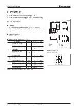
UP05C8B

Silicon NPN epitaxial planar type (Tr)

Silicon epitaxial planar type (CCD load device)

For CCD output circuits

 Features

 Two elements incorporated into one package (Tr + CCD load device)

 Costs can be reduced through downsizing of the equipment and reduction of 

the number of parts.

 Basic Part Number

 2SC3931 

+

 CCD load device

 Absolute Maximum Ratings  

T

a

 = 25

°

C

Parameter

Symbol

Rating

Unit

Tr

Collector-base voltage 
(Emitter open)

V

CBO

30

V

Collector-emitter voltage 
(Base open)

V

CEO

20

V

Emitter-base voltage 
(Collector open)

V

EBO

3

V

Collector current

I

C

15

mA

CCD
load
device

Limiting element voltage

V

max

40

V

Limiting element current

I

max

10

mA

Overall

Total power dissipation 

*

P

T

125

mW

Junction temperature

T

j

125

°

C

Storage temperature

T

stg

–55 to +125

°

C

Note) * : Measuring on substrate at 17 mm 

×

 10 mm 

×

 1 mm

Marking Symbol: 4F

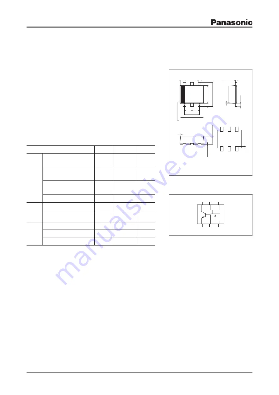
Internal Connection

3

(G)

(S)

4

1

(E)

2

(B)

(C)

6

(D)

5

Tr

FET

Unit: mm

1:  Emitter 

4:  Source

2:  Base 

5:  Drain

3:  Gate 

6:  Collector


    SSMini6-F1 Package

(0.30)

0.10

±

0.02

6

5

4

1

2

3

5

°

5

°

0.20

+0.05

–0.02

1.6

0

±

0.05

0.55

±

0.05

0.10

 max

.

0 to 0.0

2

(0.20

)

1.60

±

0.05

1

番ピン端子表示

1.2

0

±

0.05

(0.20

)

1.00

±

0.05

(0.50)(0.50)

Summary of Contents for Multi Chip Discrete UP05C8B

Page 1: ...Emitter open VCBO 30 V Collector emitter voltage Base open VCEO 20 V Emitter base voltage Collector open VEBO 3 V Collector current IC 15 mA CCD load device Limiting element voltage Vmax 40 V Limiting element current Imax 10 mA Overall Total power dissipation PT 125 mW Junction temperature Tj 125 C Storage temperature Tstg 55 to 125 C Note Measuring on substrate at 17 mm 10 mm 1 mm Marking Symbol ...

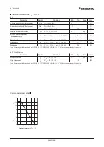
Page 2: ... VCB 6 V IE 1 mA f 200 MHz 640 MHz Noise figure NF VCB 6 V IE 1 mA f 100 MHz 3 3 dB Power gain GP VCB 6 V IE 1 mA f 100 MHz 24 dB Note Measuring methods are based on JAPANESE INDUSTRIAL STANDARD JIS C 7030 measuring methods for transistors CCD Load Device Parameter Symbol Conditions Min Typ Max Unit Pinchi off current IP VDS 10 V VG 0 3 5 5 5 mA Output impedance ZO VDS 10 V VG 0 0 05 MW Note Measur...

Page 3: ...5 C 25 C 1 10 100 20 120 80 100 60 40 140 0 UP05C8B_hFE IC Forward current transfer ratio h FE Collector current IC mA Ta 85 C 25 C 25 C 0 0 4 0 2 0 8 0 6 1 0 0 35 40 30 45 5 10 20 25 15 Collector current I C mA Base current IB mA UP05C8B_IC VCE VCE 6 V 0 0 4 0 6 0 2 1 2 0 8 1 0 1 4 0 40 50 10 20 30 Collector current I C mA Base emitter voltage VBE V UP05C8B_IC VBE VCE 6 V Ta 85 C 25 C 25 C IP VDS...

Page 4: ...ard applications intended 4 The products and product specifications described in this book are subject to change without notice for modification and or im provement At the final stage of your design purchasing or use of the products therefore ask for the most up to date Product Standards in advance to make sure that the latest specifications satisfy your requirements 5 When designing your equipmen...

Reviews: