background image

S


D


D


0


0


0


2


6


A


E


M

MN


6


6


2


7


8


5


T


B


U


C


D


7

0
0
1
1


D


6

0
1
0
1


D


5

0
0
0
0
1
1
1
1


D


4

0
0
1
1
0
0
1
1


D


3

0
1
0
1
0
1
0
1


D


2

0
0
0
0
1
1
1
1


D


1

0
0
1
1
0
0
1
1


D


0

0
1
0
1
0
1
0
1


Setting of the focus gain-up amount at vibration

Scale factor 

:×

 1.0

(0 dB)

Scale factor 

:×

 1.125 (

1.0 dB)

Scale factor 

:×

 1.25

(

1.9 dB)

Scale factor 

:×

 1.375 (

2.8 dB)

Scale factor 

:×

 1.5

(

3.5 dB)

Scale factor 

:×

 1.625 (

4.2 dB)

Scale factor 

:×

 1.75

(

4.9 dB)

Scale factor 

:×

 2.0

(

6.0 dB)

Setting of the tracking gain-up amount at vibration

Scale factor 

:×

 1.0

(0 dB)

Scale factor 

:×

 1.125 (

1.0 dB)

Scale factor 

:×

 1.25

(

1.9 dB)

Scale factor 

:×

 1.375 (

2.8 dB)

Scale factor 

:×

 1.5

(

3.5 dB)

Scale factor 

:×

 1.625 (

4.2 dB)

Scale factor 

:×

 1.75

(

4.9 dB)

Scale factor 

:×

 2.0

(

6.0 dB)

Setting of the gain-up time at vibration

Time 

  23.2 ms

Time 

  46.4 ms

Time 

  92.9 ms

Time 

185.8 ms


T


a


b


l


e


7


-


1


-


4


(


7


)

Note)

The gain-up amount set by VSET is valid only when FC2 or FR2 for the focus system or 

             TC2 or TR2 for the tracking system is written after VSET setting.

(No operation is performed to set servo parameters in the anti-vibration mode only by VSET setting.)

F


u


n


c


t


i


o


n


(


:


S


e


t


t


i


n


g


a


t


r


e


s


e


t


)

D


a


t


a


(


D


7


t


o


D


0


)

Command (HEX)

(B7 to B0)

11


F


2

A


d


d


r


e


s


s


(


H


E


X


)


(


A


7


t


o


A


0


)

(


D


)


S


e


t


t


i


n


g


f


o


r


a


n


t


i


-


v


i


b


r


a


t


i


o


n


(


V


S


E


T


)


T


h


e


g


a


i


n


-


u


p


a


m


o


u


n


t


a


n


d


g


a


i


n


-


u


p


t


i


m


e


c


a


n


b


e


s


e


t


w


h


e


n


V


D


E


T


i


s


s


e


t


t


o


"


H


.


"


(


V


D


E


T


c


a


n


b


e


m


o


n


i


t


o


r


e


d


t


h


r


o


u


g


h


t


h


e


E


X


T


1


p


i


n


.


R


e


f


e


r


t


o


7


-


1


(


5


)


(


I


)


f


o


r


d


e


t


a


i


l


s


.


)

28

Maintenance/ 

Discontinued 

Maintenance/Discontinued includes following four Product lifecycle stage.

(planed maintenance type, maintenance type, planed discontinued typed, discontinued type)

Summary of Contents for MN662785TBUC

Page 1: ...lation Subcode data processing Q data CRC check On chip Q data register On chip CD TEXT data register CIRC error correction C1 decoder double error correction C2 decoder triple error correction On chip de interleaving 16K RAM Audio data interpolation processing 4 sampling linear interpolation and previous value hold Soft muting Digital attenuation 256 levels 48 dB to 0 dB 256 levels Soft attenuati...

Page 2: ...6M DRAM 4M 4 bits 1 4M DRAM 1M 4 bits 2 4M DRAM 1M 4 bits 1 1M DRAM 256K 4 bits 2 1M DRAM 256K 4 bits 1 Others Disc rotation synchronous playback jitter free mode 2 M a i n t e n a n c e D i s c o n t i n u e d M a i n t e n a n c e D i s c o n t i n u e d i n c l u d e s f o l l o w i n g f o u r P r o d u c t l i f e c y c l e s t a g e p l a n e d m a i n t e n a n c e t y p e m a i n t e n a n...

Page 3: ...S R M O N 2 I P F L A G C L V S F L A G S R M O N 1 T M O D 2 T M O D 1 F S E L A V D D 1 O U T R A V S S 1 O U T L A V S S 2 A V D D 2 V C O F P L L F D R F D S L F A D P V C C 40 39 38 37 36 35 34 33 32 31 30 29 28 27 26 25 24 23 22 21 M N 6 6 2 7 8 5 T B U C 61 62 63 64 65 66 67 68 69 70 71 72 73 74 75 76 77 78 79 80 60 59 58 57 56 55 54 53 52 51 50 49 48 47 46 45 44 43 42 41 1 2 3 4 5 6 7 8 9 ...

Page 4: ...D 3 V A 9 t o A 0 D 3 t o D 0 N C A S 0 N C A S 1 N R A S N W E D M U T E S R D A T A 1 O U T L O U T R A V D D 1 A V S S 1 A R F D R F I R E F D S L F P L L F V C O F C S E L X 1 X 2 F S E L P M C K I P F L A G C L V S S M C K S T A T M D A T A M C L K T X T C L K 2 M L D FE TE RFENV ADPVCC A D C O N V E R T E R PWM EXT0 ISRDATA SRMON2 EXT1 ILRCK VDET PCK EXT2 IBCLK EFM BLKCK DQSY1 SUBC SSYNC TXT...

Page 5: ...t 0 DRAM address signal output 1 DRAM address signal output 2 DRAM address signal output 3 Ground for digital circuits Power supply for digital circuits Spindle motor drive signal output 1 2 3 4 5 6 7 8 9 10 11 12 13 14 15 16 17 18 19 20 21 22 DVDD3V D0 D1 NWE NRAS D2 D3 NCAS0 NCAS1 A8 A7 A6 A5 A4 A9 A0 A1 A2 A3 I I O I O O O I O I O O O O O O O O O O O O O I I O 6 PIN DESCRIPTIONS No Symbol I O F...

Page 6: ...ck RF detection signal input L Detect Dropout signal input H Dropout Laser ON signal output H ON RF signal input Reference current input A D converter reference voltage input DSL loop filter DSL bias PLL loop filter Jitter free VCO loop filter Power supply for analog circuits For DSL PLL VCOF DRF and A D converter Ground for analog circuits For DSL PLL VCOF DRF and A D converter No Symbol I O Func...

Page 7: ...nput External I O mode 64fS EFM monitor signal Digital audio interface signal output Microcomputer command clock signal input Microcomputer command data signal input Microcomputer command load signal input L Load Block clock signal output fBLKCK 75 Hz Normal speed playback CD TEXT sync signal output fDQSY 300 Hz Normal speed playback 48 49 50 51 52 53 54 55 56 57 58 59 60 61 62 63 64 OUTL AVSS1 OU...

Page 8: ...ng of OUTL OUTR and TX outputs Serial audio data output Status signal output CRC RESY CLVS NTTSTOP SQOK FLAG6 SENSE NFLOCK NTLOCK BSSEL ZDET SUBQ data output CD TEXT data output Anti shock memory controller reading data Disc rotation speed data Reset input L Reset DMUTE SRDATA1 STAT NRST SPPOL 67 68 70 I O O O Spindle motor power control signal output PC Ground for digital circuits Power supply fo...

Page 9: ... anti shock memory controller 7 Automatic adjustment 7 2 I O timing 1 Subcode interface 2 Serial data output 3 Serial data input P10 P 12 P 13 P 14 P 18 P 19 P 46 P 55 P 60 P 62 P 61 P 62 P 63 9 M a i n t e n a n c e D i s c o n t i n u e d M a i n t e n a n c e D i s c o n t i n u e d i n c l u d e s f o l l o w i n g f o u r P r o d u c t l i f e c y c l e s t a g e p l a n e d m a i n t e n a n...

Page 10: ...tion 33 8688 MHz system clock Function to select a microcomputer interface input noise filter with a command Clock selection function for microcomputer 4 MHz 8 MHz Function to select current rate of PLL frequency comparison and phase comparison Function to select output width when detecting 12T or 5T Subcode Q data adding function in control of digital audio interface output when the anti shock me...

Page 11: ...ut added PCK signal output added VDET signal output added Added function to stop A D converter operation with reference current shut off command Oscillation stop mode added A D converter reference voltage input pin ADPVCC pin 41 added No CD TEXT modes 1 and 3 11 M a i n t e n a n c e D i s c o n t i n u e d M a i n t e n a n c e D i s c o n t i n u e d i n c l u d e s f o l l o w i n g f o u r P r...

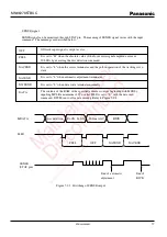
Page 12: ... B6 B5 B4 B3 B2 B1 B0 7 1 Microcomputer interface Each mode can be set by inputting the 16 bit data D15 to D0 and 8 bit command B7 to B0 starting from the MSB in 3 inputs of MDATA MCLK and MLD at the timing as shown in Figure 7 1 1 5 µs max 300 ns min 300 ns min 300 ns min 500 ns min 300 ns min 300 ns min 12 M a i n t e n a n c e D i s c o n t i n u e d M a i n t e n a n c e D i s c o n t i n u e ...

Page 13: ... Initial setting automatic adjustment and access Signal processing section Anti shock memory controller Optical servo section Control Target 13 M a i n t e n a n c e D i s c o n t i n u e d M a i n t e n a n c e D i s c o n t i n u e d i n c l u d e s f o l l o w i n g f o u r P r o d u c t l i f e c y c l e s t a g e p l a n e d m a i n t e n a n c e t y p e m a i n t e n a n c e t y p e p l a n ...

Page 14: ...6 bits 0100 1110 Turntable OFF Turntable ON Free running Acceleration Deceleration Normal play Audio control Digital audio interface control Attenuation control Spindle control PWM output control Optical servo system Playback speed control Dropout control PLL control I O control 1 DSL unbalance compensation control I O control 2 TTOFF TTON STOP ACC BRAKE PLAY Control target Symbol Function Setting...

Page 15: ...ngth Table 7 1 2 2 0111 0000 0111 0001 0111 0010 0111 0011 0111 0100 0111 0101 0111 0110 0111 0111 0111 1000 0111 1001 0111 1010 0111 1011 0111 1110 STAT output CRC STAT output RESY STAT output CLVS STAT output NTTSTOP STAT output SQOK STAT output switching STAT output BSSEL STAT output FCLV STAT output SSTAT STAT output SUBQ SQCK sync STAT output SUBQ MCLK sync STAT output ZDET Zero data detectio...

Page 16: ...10 010X 1110 0110 1110 0111 1110 1000 1110 1001 1110 1010 1110 1011 1110 11XX 1111 0000 16 bits 1111 0001 16 bits 1111 0011 16 bits 1111 0010 8 bits 1111 0100 1111 0101 1111 0110 1111 0111 1111 1000 1111 1001 1111 1010 1111 1011 1111 1100 1111 1101 1111 1110 1111 1111 Optical servo Traverse servo Access Data setting Initial setting Automatic adjust ment SENSE signal OFT FESL FESL OFT Unchanged Unc...

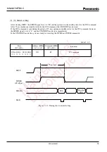
Page 17: ...mmand It is set to L when the access terminates and the pull in operation of the tracking servo starts It is set to L when automatic adjustment terminates It is set to L when data write terminates normally The contents of the RAM of the specified address is output beginning with MSB by inputting MCLK a minimum of 25 µs after MLD is set to L with the data read command DTSM sent out for data reading...

Page 18: ...mode the system is ready for receiving the DTMS and DTSM commands Data Address HEX Command HEX D7 to D0 A7 to A0 B7 to B0 D7 D6 D5 D4 D3 D2 D1D0 XX X X X X X X X X SYS command F5 Table 7 1 3 NRST SENSE STATpin MDATA MLD SYS Other than SYS 75 ms max Figure 7 1 3 Timing chart in initial setting Function 18 M a i n t e n a n c e D i s c o n t i n u e d M a i n t e n a n c e D i s c o n t i n u e d i ...

Page 19: ...ings F Various settings for optical servo system G Access command setting Note Use the DTMS command in the STANDBY or PLAY mode If you write data successively wait at least 25 µs before each data writing so that the microcomputer finishes DSP processing and becomes ready for writing next data MDATA format 1 1 1 1 0 0 1 0 A7 A6 A5 A4 A3 A2 A1 A0 D7 D6 D5 D4 D3 D2 D1 D0 Data Address Label specified ...

Page 20: ...cified 1 1 1 1 0 1 0 0 Command DTSM MDATA format Figure 7 1 4 Timing chart for reading data Min 25 µs SENSE MCLK MLD MDATA DTSM Indefinite Data 7 Data 6 Data 5 Data 4 Data 3 Data 2 Data 1 Data 0 STAT pin Note Perform either in the STANDBY or PLAY mode 20 M a i n t e n a n c e D i s c o n t i n u e d M a i n t e n a n c e D i s c o n t i n u e d i n c l u d e s f o l l o w i n g f o u r P r o d u c...

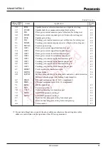
Page 21: ... TR2 Tracking low band compensation constant at vibration 10 GSET Gain crossover setting 11 VSET Mode selection for anti vibration 12 SET0 System settings 13 SET1 System settings 14 SET2 System settings 16 FES Focus gain disturbance amplitude 17 TES Tracking gain disturbance amplitude 18 CRAM2 Focus search amplitude 19 SD Search direction 1A KS Kick speed Kick brake timing 1B TVG Traverse gain con...

Page 22: ...king gain constant lower limit exponent part 49 SETKC Track count noise elimination width 4A SETTB System settings 4B KCCNT Inverted pulse width with tracking brake and servo control turned on Initial accelerating time with tracking brake turned on 6C FMAX FE signal maximum value 8 bit 2 s complement 6D FMIN FE signal minimum value 8 bit 2 s complement 78 KICK KICK output level 79 TRV Traverse out...

Page 23: ...nce constant FBAL 0 8 bit 2 s complement 128 to 127 Focus offset constant FOFS 0 8 bit 2 s complement 128 to 127 Tracking gain constant TG0 150 8 bit mantissa 1 to 255 Tracking gain constant TEXP0 1 8 bit exponent 0 to 7 Note Tracking gain constant mantissa 28 TEXP0 Tracking balance constant TBAL 0 8 bit 2 s complement 128 to 127 Tracking offset constant TOFS 0 8 bit 2 s complement 128 to 127 Dist...

Page 24: ...directly with the microcomputer command Configuration C G X Y R Z N Z 1 K fs of the focus system 88 2 kHz fs of the tracking system 88 2 kHz fs of the filter for low band compensation 44 1 kHz N in Z N can be replaced with 2 or 1 by setting bit 1 of SET0 in case of the focus system 1 in case of the tracking system 1 G Z G 1 C Z N 1 Z 1 TG G or 28 TEXP FG TR R or 2 15 FR 2 15 TC C or 128 FC 128 K 1...

Page 25: ...ts 1 to 127 Tracking low band compensation constant at 64 vibration TR2 8 bits 1 to 127 D6 D6 D6 D6 D6 D6 D6 D6 D7 D7 D7 D7 D7 D7 D7 D7 D5 D5 D5 D5 D5 D5 D5 D5 D4 D4 D4 D4 D4 D4 D4 D4 D3 D3 D3 D3 D3 D3 D3 D3 D2 D2 D2 D2 D2 D2 D2 D2 D1 D1 D1 D1 D1 D1 D1 D1 D0 D0 D0 D0 D0 D0 D0 D0 08 09 0A 0B 0C 0D 0E 0F Data D7 to D0 Command HEX B7 to B0 Function Setting at reset F2 Address HEX A7 to A0 25 M a i n ...

Page 26: ...B and type C They can be selected by setting SET2 The dead zone width can be specified by setting DED0 26 M a i n t e n a n c e D i s c o n t i n u e d M a i n t e n a n c e D i s c o n t i n u e d i n c l u d e s f o l l o w i n g f o u r P r o d u c t l i f e c y c l e s t a g e p l a n e d m a i n t e n a n c e t y p e m a i n t e n a n c e t y p e p l a n e d d i s c o n t i n u e d t y p e d ...

Page 27: ...0 1 1 0 0 1 1 0 0 D0 1 0 1 0 1 0 1 0 1 0 1 0 1 0 1 0 Setting for tracking system Table 7 1 4 6 Focus gain at the disturbance frequency of 750 Hz Approx value 3 92 dB Approx value 3 36 dB Approx value 2 80 dB Approx value 2 24 dB Approx value 1 68 dB Approx value 1 12 dB Approx value 0 56 dB Approx value 0 dB Approx value 1 05 dB Approx value 2 11 dB Approx value 3 16 dB Approx value 4 21 dB Approx...

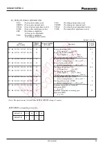
Page 28: ...cale factor 1 625 4 2 dB Scale factor 1 75 4 9 dB Scale factor 2 0 6 0 dB Setting of the gain up time at vibration Time 23 2 ms Time 46 4 ms Time 92 9 ms Time 185 8 ms Table 7 1 4 7 Note The gain up amount set by VSET is valid only when FC2 or FR2 for the focus system or TC2 or TR2 for the tracking system is written after VSET setting No operation is performed to set servo parameters in the anti v...

Page 29: ...8 bit mantissa 1 to 255 Focus gain constant at vibration FEXP2 2 8 bit exponent 1 to 7 Focus gain constant mantissa 28 FEXP2 Tracking gain constant at vibration TG2 150 8 bit mantissa 1 to 255 Tracking gain constant at vibration TEXP2 1 8 bit exponent 1 to 7 Tracking gain constant mantissa 28 TEXP2 Table 7 1 4 8 29 M a i n t e n a n c e D i s c o n t i n u e d M a i n t e n a n c e D i s c o n t i...

Page 30: ...X X X X X D6 0 1 X X X X X X D5 0 0 1 1 X X X X X X X X D4 0 1 0 1 X X X X D3 0 0 1 1 X X X X X X X X D2 0 1 0 1 X X X X X X X X X X X X X X X X X X X X 1 1 1 1 1 1 1 1 1 1 1 1 12 F2 Function Setting at reset Data D7 to D0 Command HEX B7 to B0 Address HEX A7 to A0 X X X X X X X X X X X X D1 0 1 1 1 Setting the number of Fo loop filter delay stages 2nd order Z 2 1st order Z 1 30 M a i n t e n a n c...

Page 31: ...od With vibration Without vibration Focus offset adjustment method direction Same as MN66271 direction Wait time after TCNT 50 ms 100 ms 0 ms 10 ms DAC output limiter FABC TABC OFF ON F2 13 E 2 SET1 setting Table 7 1 4 10 Function Setting at reset Data D7 to D0 Command HEX B7 to B0 Address HEX A7 to A0 Note It is recommended to turn off the high speed kickback function while the anti shock memory ...

Page 32: ... 1 4 1 32 1 16 Disc detection focus rough gain adjustment frequency 5 4 Hz 2 6 Hz Traverse intermittent drive Output enabled Output disabled F2 14 E 3 SET2 setting Table 7 1 4 11 Function Setting at reset Data D7 to D0 Command HEX B7 to B0 Figure 1 Traverse dead zone amp Type A Figure 2 Traverse dead zone amp Type B Figure 3 Traverse dead zone amp Type C Address HEX A7 to A0 DED0 DED0 2 DED0 2 Not...

Page 33: ...ustment time 134 ms 319 ms Focus search mode Conventional mode Amplitude 1 4 Focus balance adjustment output Positive polarity Conventional mode Negative polarity Focus search frequency 1 3 Hz 2 6 Hz F2 E 4 SET3 setting Table 7 1 4 12 Function Setting at reset Data D7 to D0 Command HEX B7 to B0 1E Address HEX A7 to A0 33 M a i n t e n a n c e D i s c o n t i n u e d M a i n t e n a n c e D i s c o...

Page 34: ...2 D7 to D4 0 to 7 F2 X X X X D3 D2 D1 D0 Function D7 D6 D5 D4 X X X X D7 D6 D5 D4 X X X X X X X X D3 D2 D1 D0 7C 7D Data D7 to D0 Address HEX A7 to A0 Command HEX B7 to B0 See next page for the setting of vibration detection level Sampling frequency for filter arithmetic operation 11 02 kHz Table 7 1 4 13 Setting at reset 3 1 5 5 34 M a i n t e n a n c e D i s c o n t i n u e d M a i n t e n a n c...

Page 35: ...T 128 to 255 Function Data D7 to D0 Address HEX A7 to A0 Command HEX B7 to B0 Table 7 1 4 14 Setting at reset 230 35 M a i n t e n a n c e D i s c o n t i n u e d M a i n t e n a n c e D i s c o n t i n u e d i n c l u d e s f o l l o w i n g f o u r P r o d u c t l i f e c y c l e s t a g e p l a n e d m a i n t e n a n c e t y p e m a i n t e n a n c e t y p e p l a n e d d i s c o n t i n u e d...

Page 36: ...unting countermeasure for focus balance adjustment No Yes Data D7 to D0 Address HEX A7 to A0 Command HEX B7 to B0 4A F2 Function Setting at reset 36 M a i n t e n a n c e D i s c o n t i n u e d M a i n t e n a n c e D i s c o n t i n u e d i n c l u d e s f o l l o w i n g f o u r P r o d u c t l i f e c y c l e s t a g e p l a n e d m a i n t e n a n c e t y p e m a i n t e n a n c e t y p e p l...

Page 37: ...mmand HEX B7 to B0 Address HEX A7 to A0 Table 7 1 4 16 E 8 Software reset Accessing the data in AAh address initializes servo processing DSP processing starts from the top address X X X X X X X X AA F2 Software reset Data is disabled Function Data D7 to D0 Command HEX B7 to B0 Address HEX A7 to A0 Note Only the digital servo section is reset in the software reset operation Table 7 1 4 17 37 M a i ...

Page 38: ...teaching of the maximum and minimum values FMAX and FMIN of the FE signal will be however conducted The focus will be pulled in when the S shape signal is detected after the first excitation period Once the focus is pulled in the servo DSP automatically sets SD D2 to 1 Then the focus will be pulled in when the S curve signal is detected after the first peak of excitation After offset and focus bal...

Page 39: ...e adjustment mode Table 7 1 4 20 Disturbance amplitude one side 36 8 bit data 0 to 127 Amplitude of the disturbance waves injected in the tracking balance adjustment mode is set Actual disturbance amplitude is 1 8 CRAM4 Address HEX A7 to A0 Address HEX A7 to A0 Data D7 to D0 Data D7 to D0 Setting at reset 39 M a i n t e n a n c e D i s c o n t i n u e d M a i n t e n a n c e D i s c o n t i n u e ...

Page 40: ...etting 1 count TS delay Setting value 0 No delay OFT TE KICK Delay Brake 1 4 track OFT TE KICK When OFT is turned to L before reaching a position of 1 4 track When OFT is turned to L after passing the position of 1 4 track Delay Brake Address HEX A7 to A0 TS 11 3 ms Data D7 to D0 40 M a i n t e n a n c e D i s c o n t i n u e d M a i n t e n a n c e D i s c o n t i n u e d i n c l u d e s f o l l ...

Page 41: ...n the TE slope is inverted and reaches the level of the SETKC it is regarded that the TE slope has actually changed Function F2 Table 7 1 4 23 Table 7 1 4 24 Address HEX A7 to A0 Function Address HEX A7 to A0 Command HEX B7 to B0 Command HEX B7 to B0 SETKC TE Ignored SETKC Function Address HEX A7 to A0 Command HEX B7 to B0 15 Data D7 to D0 Data D7 to D0 Data D7 to D0 Setting at reset Setting at re...

Page 42: ...o 127 65 F 10 Traverse output gain setting TRV 79 0 D6 D5 D4 D3 D2 D1 D0 F2 Function Command HEX B7 to B0 F2 Table 7 1 4 26 Table 7 1 4 27 Function Command HEX B7 to B0 Address HEX A7 to A0 Address HEX A7 to A0 TS 11 3 µs Function Command HEX B7 to B0 Address HEX A7 to A0 Data D7 to D0 Data D7 to D0 Data D7 to D0 Setting at reset Setting at reset Setting at reset 42 M a i n t e n a n c e D i s c o...

Page 43: ...xponent 0 to 7 Upper limit GLF1 28 GLF2 Focus gain lower limit GLF3 mantissa 128 to 255 GLF4 exponent 0 to 7 Lower limit GLF3 28 GLF4 143 144 Table 7 1 4 29 Table 7 1 4 30 F 11 Traverse fine adjustment gain setting TRVG0 Table 7 1 4 28 F2 37 D7 D6 D5 D4 D3 D2 D1 D0 Traverse gain 0 to 127 TRVG0 16 18 Set the above value after setting the TRV value Function Command HEX B7 to B0 Address HEX A7 to A0 ...

Page 44: ...track count means the number of tracks until the brake operation start point is reached Function Command HEX B7 to B0 TE sampling frequency in track counting is 176 4 kHz Care must be taken so that the maximum TE frequency in track counting does not exceed one fourth of the sampling frequency Data D15 to D0 44 M a i n t e n a n c e D i s c o n t i n u e d M a i n t e n a n c e D i s c o n t i n u ...

Page 45: ...loss compensation value Table 7 1 4 33 D1 D0 2C The shaft loss compensation value will be enabled only when the spindle is in free running condition STOP No compensation will be enabled with this value set to 0 Function Data D7 to D0 Address HEX Command HEX A7 to A0 B7 to B0 Function Data D7 to D0 Address HEX Command HEX A7 to A0 B7 to B0 Function F2 F2 H 1 Setting of spindle forced acceleration d...

Page 46: ...1 X X X X X X X X X X X X X X X X X X X X X X X 0 1 X X X X X X X X BIMAIN BISUB INV MEMP DEPSEL SMUTE LRINV XBS ASC LIVE AUDIO1 AUDIO2 XMUTE MMUTE X X X X X X X X X X X X X X X 0 1 X X X X X X X X X X X X X X X X X X X X X X X 0 1 X X X X X X X X X X X X X X X X X X X X X X X 0 1 X X X X X X X X X X X X X X X X X X X X X X X 0 1 X X X X X X X X X X X X X X X X X X X X X X 0 1 1 X X X X X X X X X ...

Page 47: ... mode Not defined X X X X X X X X X X X X X X X X X X X X X X X X X X X X X X X X X X X X X X X X X X X X X X X X X X X X X X X X X X X X X X X X X X X X X X X X X X X X X X X X X X X X X X X X X X X X 42 X X X X X X X X X X X X X X X X X X X 0 0 1 1 X X X X X X X X X X X X X X X X X X X 0 1 0 1 X X X X X X X X X X X X X X X X X 0 1 X X X X UBITC COPYI TXVSEL TMUTE IPDISEN TXDSEL VFREE XSEL CATC C...

Page 48: ...reset and stops X X X X X X X X X X X X X X X X X X 0 1 X X X X X X X X X X X X X X X X 0 1 X X X X X X X X X X X X X X X X 0 1 X X X X 0 0 0 0 0 0 0 0 0 0 0 0 0 0 0 0 0 0 0 0 45 X X X X X X X X X X X X 0 1 X X X X X X 0 0 0 0 0 0 0 0 0 0 0 0 0 0 0 0 0 0 0 0 X X X X X X X X X X 0 1 X X X X X X X X FO1SEL FO2SEL SG0 SG1 PCINV CLVSEL JFMODE ACCFIX KILL CKSTOP X X X X X X X X 0 1 X X X X X X X X X X ...

Page 49: ...X X X X X X X X X X X X X X X X X X X X X X X X X X X X X X FBAL1E FBAL2E TBAL1E TBAL2E MCFSEL X X X X X X X X X X X X X X X X X X 0 1 X X X X X X X X X X 0 0 0 0 0 0 0 0 0 0 0 0 0 0 0 0 0 0 0 0 X X X X 0 0 1 1 X X X X X X 0 1 0 1 X X 0 1 0 1 X X X X X X 0 0 1 1 X X X X X X 49 M a i n t e n a n c e D i s c o n t i n u e d M a i n t e n a n c e D i s c o n t i n u e d i n c l u d e s f o l l o w i ...

Page 50: ...X X X X X X X 0 1 X X X X X X X X X X X X 0 1 X X X X X X X X X X X X X X X X X X 0 1 X X X X X X X X X X X X X X DSL s DO processing Enabled Disabled Spindle s DO processing Enabled Disabled PLL s DO processing Enabled Disabled DO with faults processing Enabled Disabled X X X X X X X X X X X X X X X X X X X X X X X X X X X X X X X X 4A X X X X X X X X X X X X X X X X X X X X X X X X DSLDO CLVDO P...

Page 51: ...0 0 0 0 0 0 0 0 0 X X X X X X X X X X X X X X X 0 1 X X X X X X X X X X X X X X X X X X X X X X X X X X X X X X X X X X X X X X 0 1 X X X X X X X X X X X X X X X X X X D9 X X X X X X X X PLLG1 PLLG2 PCKG IROFF PLHLD DET5T FL02 FL04 FL08 FL16 FH32 PLLG PLLG3 PLLG4 X X X X X X X X X X X X D8 X X X X X X X X X X X X X X X X X X X X D7 X X X X X X X X X X X X X X X X X X X X D6 X X X X X X X X X X X X...

Page 52: ...B7 to B0 Function Setting at reset X X X X X X X X X X X X X X X X X X X X X X X X X X X X X X X X X X X X X X X X 0 0 0 0 0 0 0 0 1 1 1 1 1 1 1 1 DSLBSEL DSLB1E DSLB2E DSLBEN X X X X X X 0 1 X X 0 0 1 1 X X X X 0 1 0 1 X X X X X X X X X X X X X X X X X X 0 1 X X X X X X X X X X X X X X 0 0 0 0 0 0 0 0 X X X X X X X X 4D Symbol Data D15 to D0 Command HEX B7 to B0 Function Setting at reset EFM or S...

Page 53: ... pin fixed at low level Disabled Enabled Note 1 Enabled pins SRDATA LRCK BCLK IPFLAG SUBC NCLDCK Note 2 Serial input mode is activated if IOSTOP is disabled EXT0 EXT1 EXT2 RDATA LRCK BCLK SMCK frequency selection 8 4672 MHz DF input selection Input bypassing the anti shock memory controller Input from the anti shock memory controller Off track noise filter Disabled Enabled EXT0 pin selection Norma...

Page 54: ...nction Setting at reset STAT pin output selection CRC RESY CLVS NTTSTOP SQOK BSSEL FCLV SUBQ SQCK sync TXTDAT SUBQ MCLK sync TXTDAT ZDET Zero data detection STAT pin output setting STAT pin output 0 FLAG6 0 SENSE 0 NFLOCK 0 NTLOCK STAT pin output mode selection by MCLK excluding the setting of SENSE 01 1 FLAG6 2 SENSE 3 NFLOCK 4 NTLOCK 5 SQOK 6 CRC 7 CLVS 8 NTTSTOP Clearing FLAG6 output from STAT ...

Page 55: ... X X X X X X X X X X X X X X X 0 1 X X 0 1 X X 0 1 X X X X EXT0ST EXT1ST EXT2ST 81 Memory system stop Memory system run Q data disabled Q data enabled Comparison connection aborted Direct connection 2 pair comparison connection 3 pair comparison connection Normal operation Read address reset Decoding aborted Decoding executed Normal operation Write address reset Encoding aborted Encoding executed ...

Page 56: ...parison Parameter reset at start of encoding during direct connection No Yes X X X X X X X X X X X X X X 0 1 X X X X X X X X X X X X X X 0 1 X X X X X X X X X X X X 0 0 1 1 X X X X X X 0 1 X X X X X X 0 1 0 1 X X X X X X X X X X X X 0 1 0 0 0 0 0 0 0 0 0 0 X X X X 0 1 X X X X X X X X X X X X X X 0 1 0 0 0 0 X X X X X X X X 0 1 X X X X X X X X 1 1 1 1 1 1 1 1 1 1 CMOD RSEL1 RSEL0 WSEL C2SEL CMPSEL ...

Page 57: ...code is input the previous value will be kept on hold and bit U will be output At that time CRC data is added with disabling data Note2 Interruption is not allowed while the Q code is input otherwise the wrong bit U will be output The Q code cannot be input into a single block more than once otherwise the wrong bit U will be output Command HEX B7 to B0 Data Symbol Function Output timing 16 clocks ...

Page 58: ...rflow Figure 7 1 6 Timing chart for reading data Min 25 µs MCLK MLD Read command STAT pin S0 S1 S4 S0 S1 MDATA Function Command HEX B7 to B0 Symbol Output bit 90 91 58 M a i n t e n a n c e D i s c o n t i n u e d M a i n t e n a n c e D i s c o n t i n u e d i n c l u d e s f o l l o w i n g f o u r P r o d u c t l i f e c y c l e s t a g e p l a n e d m a i n t e n a n c e t y p e m a i n t e n ...

Page 59: ...sion I O port Table 7 1 6 8 Expansion I O port EXT2 input data Expansion I O port EXT1 input data Expansion I O port EXT0 input data EXT2RD EXT1RD EXT0RD S5 S6 S7 Function Symbol 93 Output bit Command HEX B7 to B0 59 M a i n t e n a n c e D i s c o n t i n u e d M a i n t e n a n c e D i s c o n t i n u e d i n c l u d e s f o l l o w i n g f o u r P r o d u c t l i f e c y c l e s t a g e p l a n...

Page 60: ... input amount for the fine AGC The gain will be unchanged Inputs the disturbance into the focus servo loop and adjusts the gain crossover to the frequency set by the microcomputer command Inputs the disturbance into the tracking servo loop and adjusts the gain crossover to the frequency set by the microcomputer command Offset AOC1 Note Fo balance ABC1 Tr balance ABC2 F9 F7 FB FC FD FE FF FWD REV e...

Page 61: ...RC SQCK NCLDCK BLKCK H CRC OK L CRC NG SUBQ CRC 8 7 ms CRC 80 clocks Q4 Q79 Q80 Q1 Q2 Q3 61 M a i n t e n a n c e D i s c o n t i n u e d M a i n t e n a n c e D i s c o n t i n u e d i n c l u d e s f o l l o w i n g f o u r P r o d u c t l i f e c y c l e s t a g e p l a n e d m a i n t e n a n c e t y p e m a i n t e n a n c e t y p e p l a n e d d i s c o n t i n u e d t y p e d d i s c o n t ...

Page 62: ...ing SBCK the content of FLAG output will vary So measuring the error rate while reading subcode is not possible Take it into consideration when designing the system Typ Typ 136 µs 1 6 µs BLKCK SBCK SUBC S0 S1 P1 to W1 P2 to W2 P3 to W3 P4 to W4 P5 to W5 P6 to W6 P7 to W7 NCLDCK SBCK NCLDCK SUBC P Q R S T U V W Figure 7 2 2 NCLDCK SUBC and SBCK timing chart Refer to the values specified in the PROD...

Page 63: ...X X X X X X X Symbol Data D15 to D0 Command HEX B7 to B0 Symbol Table 7 3 2 2 Data D15 to D0 Command HEX B7 to B0 Symbol C Serial data output selection The following command determines whether serial data in serial data output mode 1 or serial data output mode 2 is output with or without attenuation and de emphasis Data D15 to D0 Command HEX B7 to B0 Table 7 3 3 With no attenuation or de emphasis ...

Page 64: ... data output mode 1 or 2 The input timing of serial data is the same as the output timing of serial data SRDATA LRCK BCLK Invalid 1413121110 9 8 7 6 5 4 3 2 1 0 15 1413121110 9 8 7 6 5 4 3 2 1 0 15 15 L ch R ch L ch Invalid Invalid D Serial data output timing 7 2 3 Serial data input 64 M a i n t e n a n c e D i s c o n t i n u e d M a i n t e n a n c e D i s c o n t i n u e d i n c l u d e s f o l...

Page 65: ...nd and used at the same voltage Note 3 Each of DVDD1 DVDD2 AVDD1 and AVDD2 pins should be directly connected to the specified power supply and used at the same voltage Note 4 DVDD1 DVDD2 AVDD1 and AVDD2 should be powered up at the same time Note 5 The operation of the audio D A converter is not guaranteed for operations in 2x speed playback modes i e when anti shock memory controller is not operat...

Page 66: ...age as DVDD Self excited Oscillation Note 8 Ta 40 C to 85 C DVSS1 2 0 V AVSS1 2 0 V Audio system supply voltage Analog system supply voltage Note 7 Crystal frequency External capacitance 1 External capacitance 2 Note 8 Oscillator Circuit Note 7 V B4 3 6 DVDD3V D RAM interface voltage VDD1 2 33 8688 10 10 66 M a i n t e n a n c e D i s c o n t i n u e d M a i n t e n a n c e D i s c o n t i n u e d...

Page 67: ... mode Ta 25 C 23 76 24 80 46 152 48 160 Total power consumption Anti shock memory controller is not operating No external load in 2x speed playback mode Ta 25 C C1 C2 C3 C4 Supply current Total power consumption 67 M a i n t e n a n c e D i s c o n t i n u e d M a i n t e n a n c e D i s c o n t i n u e d i n c l u d e s f o l l o w i n g f o u r P r o d u c t l i f e c y c l e s t a g e p l a n e...

Page 68: ... OFT NRFDET BDO NTEST MCLK MDATA MLD SQCK BCLK1 TXTCLK1 DMUTE SRDATA1 NRST SBCK TXTCLK2 LRCK2 0 66 Symbol DVDD1 2 3 3 V DVSS1 2 0 V AVDD1 2 3 3 V AVSS1 2 0 V Ta 40 C to 85 C fX1 33 8688 MHz 68 M a i n t e n a n c e D i s c o n t i n u e d M a i n t e n a n c e D i s c o n t i n u e d i n c l u d e s f o l l o w i n g f o u r P r o d u c t l i f e c y c l e s t a g e p l a n e d m a i n t e n a n c...

Page 69: ...UBC TXTDAT2 SRDATA2 SBCK TXTCLK2 LRCK2 NCLDCK DQSY2 BCLK2 D0 D1 NWE NRAS D2 D3 NCAS0 NCAS1 A8 A7 A6 A5 A4 A9 A0 A1 A2 A3 2 SPOUT TRVP TRVM TRP TRM FOP FOM Output Pins 2 3 V C10 C11 Output voltage high level Output voltage low level VOH2 VOL2 DVDD1 2 0 6 0 4 V IOH2 1 mA IOL2 1 mA C12 Output leakage current ILK2 1 µA VO 0 V to 3 3 V Hi Z M a i n t e n a n c e D i s c o n t i n u e d M a i n t e n a ...

Page 70: ... 0 µA V p p µA Input leakage current ILKD Analog System Input Pin 3 DRF C16 C17 1 0 µA Internal resistance between ARF and DRF RDRF ARF 1 65 V 10 kΩ DVDD1 2 3 3 V DVSS1 2 0 V AVDD1 2 3 3 V AVSS1 2 0 V Ta 40 C to 85 C fX1 33 8688 MHz 70 M a i n t e n a n c e D i s c o n t i n u e d M a i n t e n a n c e D i s c o n t i n u e d i n c l u d e s f o l l o w i n g f o u r P r o d u c t l i f e c y c l ...

Page 71: ...te Normal current mode Normal to 2x speed jitter free mode VCO frequency for PCK switching 0 5 Analog System Output Pin 1 DSLF IREF pin is pulled up to AVDD2 by a 47 kΩ resistor Analog System Output Pin 2 PLLF IREF pin is pulled up to AVDD2 by a 47 kΩ resistor C18 C19 C20 C21 C22 C23 C24 C25 C26 C27 C28 C29 Hi Z 98 169 8 0 105 182 15 0 4 32 169 8 46 130 130 130 2 0 140 140 6 0 130 169 169 98 4 0 1...

Page 72: ...0 001 µF VARF 1 0 V p p Typ 0 022 µF 100 kΩ ARF DSLF DRF DVDD1 2 3 3 V DVSS1 2 0 V AVDD1 2 3 3 V AVSS1 2 0 V Ta 40 C to 85 C fX1 33 8688 MHz 72 M a i n t e n a n c e D i s c o n t i n u e d M a i n t e n a n c e D i s c o n t i n u e d i n c l u d e s f o l l o w i n g f o u r P r o d u c t l i f e c y c l e s t a g e p l a n e d m a i n t e n a n c e t y p e m a i n t e n a n c e t y p e p l a n ...

Page 73: ...D1 2 3 3 V DVSS1 2 0 V AVDD1 2 3 3 V AVSS1 2 0 V Ta 40 C to 85 C fX1 33 8688 MHz 73 M a i n t e n a n c e D i s c o n t i n u e d M a i n t e n a n c e D i s c o n t i n u e d i n c l u d e s f o l l o w i n g f o u r P r o d u c t l i f e c y c l e s t a g e p l a n e d m a i n t e n a n c e t y p e m a i n t e n a n c e t y p e p l a n e d d i s c o n t i n u e d t y p e d d i s c o n t i n u e ...

Page 74: ...nlinearity 2 DVDD1 2 3 3 V DVSS1 2 0 V AVDD1 2 3 3 V AVSS1 2 0 V Ta 40 C to 85 C fX1 33 8688 MHz 74 M a i n t e n a n c e D i s c o n t i n u e d M a i n t e n a n c e D i s c o n t i n u e d i n c l u d e s f o l l o w i n g f o u r P r o d u c t l i f e c y c l e s t a g e p l a n e d m a i n t e n a n c e t y p e m a i n t e n a n c e t y p e p l a n e d d i s c o n t i n u e d t y p e d d i s ...

Page 75: ...t by the external circuit gain of the application circuit and converting the result to the value at the output pin of this IC Note 12 The D A converter always operates in the normal speed playback mode 0 009 1 62 EIAJ EIAJ EIAJ EIAJ Reference input signal of 1 kHz Full scale Note 10 Vrms C43 Output level 2 0 69 0 88 1 07 C42 Output level difference Difference of OUTL and OUTR pins at output level ...

Page 76: ...p F D V S S M N 6 6 2 7 8 5 T B U C A V D D 1 O U T L A V S S 1 O U T R 0 1 µF D V D D 0 1 µF D V S S 2 A V S S 2 D V D D 2 A V D D 2 D V S S D V D D A V S S 2 A V D D 2 0 1 µF D V S S 1 D V D D 1 76 M a i n t e n a n c e D i s c o n t i n u e d M a i n t e n a n c e D i s c o n t i n u e d i n c l u d e s f o l l o w i n g f o u r P r o d u c t l i f e c y c l e s t a g e p l a n e d m a i n t e ...

Page 77: ...litude VRIP mV p p Power Supply Ripple Noise Note 14 15 C46 Ripple noise amplitude VNZ mV p p 50 Note 14 The permissible ripple and noise of power supply to this IC are guaranteed on condition that the ripple frequency range is between 50 Hz and 100 Hz the noise frequency is at 500 kHz and that both ripple and noise are sine wave signals as shown below Pay utmost attention to these ripple signal a...

Page 78: ...VDD tRA tFA tRB tFB MCLK DVDD1 2 3 3 V DVSS1 2 0 V AVDD1 2 3 3 V AVSS1 2 0 V Ta 40 C to 85 C fX1 33 8688 MHz 78 M a i n t e n a n c e D i s c o n t i n u e d M a i n t e n a n c e D i s c o n t i n u e d i n c l u d e s f o l l o w i n g f o u r P r o d u c t l i f e c y c l e s t a g e p l a n e d m a i n t e n a n c e t y p e m a i n t e n a n c e t y p e p l a n e d d i s c o n t i n u e d t y ...

Page 79: ...atch pulse width µs tLDW 0 5 Microcomputer Instruction Input Timing fMCLK 5 DVDD1 2 3 3 V DVSS1 2 0 V AVDD1 2 3 3 V AVSS1 2 0 V Ta 40 C to 85 C fX1 33 8688 MHz 79 M a i n t e n a n c e D i s c o n t i n u e d M a i n t e n a n c e D i s c o n t i n u e d i n c l u d e s f o l l o w i n g f o u r P r o d u c t l i f e c y c l e s t a g e p l a n e d m a i n t e n a n c e t y p e m a i n t e n a n c...

Page 80: ...h ns tCKH tSQH tCKL tSQL 200 200 ns C65 Delay time C66 Setup delay time ns tSBD tSQD tSD 150 150 Subcode Interface 2 FSEL H tCK tSQ 500 ns ns DVDD1 2 3 3 V DVSS1 2 0 V AVDD1 2 3 3 V AVSS1 2 0 V Ta 40 C to 85 C fX1 33 8688 MHz 80 M a i n t e n a n c e D i s c o n t i n u e d M a i n t e n a n c e D i s c o n t i n u e d i n c l u d e s f o l l o w i n g f o u r P r o d u c t l i f e c y c l e s t a...

Page 81: ... a n c e D i s c o n t i n u e d M a i n t e n a n c e D i s c o n t i n u e d i n c l u d e s f o l l o w i n g f o u r P r o d u c t l i f e c y c l e s t a g e p l a n e d m a i n t e n a n c e t y p e m a i n t e n a n c e t y p e p l a n e d d i s c o n t i n u e d t y p e d d i s c o n t i n u e d t y p e ...

Page 82: ...p Max Unit Clock width High level pulse width Low level pulse width Delay time tMT tMTH tMTL tMTD ns ns ns ns DVDD1 2 3 3 V DVSS1 2 0 V AVDD1 2 3 3 V AVSS1 2 0 V Ta 40 C to 85 C fX1 33 8688 MHz 82 M a i n t e n a n c e D i s c o n t i n u e d M a i n t e n a n c e D i s c o n t i n u e d i n c l u d e s f o l l o w i n g f o u r P r o d u c t l i f e c y c l e s t a g e p l a n e d m a i n t e n a...

Page 83: ... pulse width Delay time tMT tMTH tMTL tMTD ns ns ns ns Note 15 STAT output data switching with MCLK when using 75h command tMTD MCLK STAT tMTL tMTH tMT DVDD1 2 3 3 V DVSS1 2 0 V AVDD1 2 3 3 V AVSS1 2 0 V Ta 40 C to 85 C fX1 33 8688 MHz 83 M a i n t e n a n c e D i s c o n t i n u e d M a i n t e n a n c e D i s c o n t i n u e d i n c l u d e s f o l l o w i n g f o u r P r o d u c t l i f e c y c...

Page 84: ... tBCLKL 177 Setup time tST ns 50 D A output Interface 2 ns C88 C89 C92 ns Hold time tHD 50 2x speed playback mode BCLK1 BCLK2 SRDATA1 SRDATA2 LRCK1 LRCK2 tBCLKL tBCLKH tBCLK tST tHD VDD 3 3 V VSS 0 V AVDD 3 3 V AVSS 0 V Ta 40 C to 85 C fX1 33 8688 MHz 84 M a i n t e n a n c e D i s c o n t i n u e d M a i n t e n a n c e D i s c o n t i n u e d i n c l u d e s f o l l o w i n g f o u r P r o d u c...

Page 85: ...8 LRCK frequency IBCLK ISRDATA ILRCK 1 fBCLK tCH tCL tDSU tDH tBL tLB tBL tLB 1 fLRCK VDD 3 3 V VSS 0 V AVDD 3 3 V AVSS 0 V Ta 40 C to 85 C fX1 33 8688 MHz 85 M a i n t e n a n c e D i s c o n t i n u e d M a i n t e n a n c e D i s c o n t i n u e d i n c l u d e s f o l l o w i n g f o u r P r o d u c t l i f e c y c l e s t a g e p l a n e d m a i n t e n a n c e t y p e m a i n t e n a n c e t...

Page 86: ...ne system clock cycle which is indicated as 1 16 9344 MHz seconds C115 C116 Refresh period Playback fs 44 1 kHz Memory system ON with decode sequence executed tref tref tref tref 16 Mbits full bits ms ms ms ms 5 9 23 3 3 0 11 7 C99 C100 Parameter Symbol Conditions Limits Min Typ Max Unit 16 Mbits 4 bit compression 4 Mbits full bits 4 Mbits 4 bit compression C117 C118 tref tref ms ms 1 5 5 9 1 Mbit...

Page 87: ... A0 to A9 D0 to D3 READ NWE READ trasl trash tcash tcasl trcd trads tradh tcads tradv tcadhr Read Timing H tcadv 87 M a i n t e n a n c e D i s c o n t i n u e d M a i n t e n a n c e D i s c o n t i n u e d i n c l u d e s f o l l o w i n g f o u r P r o d u c t l i f e c y c l e s t a g e p l a n e d m a i n t e n a n c e t y p e m a i n t e n a n c e t y p e p l a n e d d i s c o n t i n u e d ...

Page 88: ...0 16 00 0 20 0 825 0 825 16 00 0 20 14 00 0 20 0 30 0 05 0 65 M 0 13 0 10 M a i n t e n a n c e D i s c o n t i n u e d M a i n t e n a n c e D i s c o n t i n u e d i n c l u d e s f o l l o w i n g f o u r P r o d u c t l i f e c y c l e s t a g e p l a n e d m a i n t e n a n c e t y p e m a i n t e n a n c e t y p e p l a n e d d i s c o n t i n u e d t y p e d d i s c o n t i n u e d t y p e ...

Page 89: ...t At the final stage of your design purchasing or use of the products therefore ask for the most up to date Product Standards in advance to make sure that the latest specifications satisfy your requirements 5 When designing your equipment comply with the range of absolute maximum rating and the guaranteed operating conditions operating power supply voltage and operating environment etc Especially ...

Reviews: