background image

15

KX-TG1032SK/KX-TGA101S

Summary of Contents for KX-TG1032SK

Page 1: ...rks Co Ltd 2010 Unauthorized copying and distribution is a violation of law ORDER NO KM41003051CE F13 Telephone Equipment Model No KX TG1032SK KX TGA101S Expandable Digital Cordless Answering System S Silver Version for U S A ...

Page 2: ...2 KX TG1032SK KX TGA101S ...

Page 3: ...asurements and Adjustments 46 11 1 Equipment Required 46 11 2 The Setting Method of JIG Base Unit 46 11 3 Adjustment Standard Base Unit 48 11 4 Adjustment Standard Charger Unit 50 11 5 The Setting Method of JIG Handset 51 11 6 Adjustment Standard Handset 53 11 7 Things to Do after Replacing IC or X tal 54 11 8 How to Check the Handset Speaker or Receiver 55 11 9 Frequency Table MHz 55 12 Miscellan...

Page 4: ... used batteries according to the instructions 2 2 About Lead Free Solder Pbf Pb free Note In the information below Pb the symbol for lead in the periodic table of elements will refer to standard solder or solder that con tains lead We will use PbF solder when discussing the lead free solder used in our manufacturing process which is made from Tin Sn Silver Ag and Copper Cu This model and others li...

Page 5: ...Bismuth Sn Zn Bi Please check the manufacturer s specific instructions for the melting points of their products and any precautions for using their product with other materials The following lead free PbF solder wire sizes are recommended for service of this product 0 3 mm 0 6 mm and 1 0 mm 2 3 Discarding of P C Board When discarding P C Board delete all personal information such as telephone dire...

Page 6: ...d specifications are subject to change without notice Note for Service Operation range Up to 300 m outdoors Up to 50 m indoors depending on the condition Analog telephone connection Telephone Line Optional headset KX TCA60 KX TCA86 KX TCA92 KX TCA93 KX TCA94 ...

Page 7: ...Speech Decoding Speech Encoding BMC Burst Decoding Burst Encoding RF Interface 18 19 TXDA RXDA 15 21 20 22 RSSI SYCL SYDA SYEN ANT1 ANT2 RF Module 18 16 2 31 8 21 14 13 12 12 13 XTAL X1 10 368 MHz EEPROM SCL SDA 6 5 To AC Adaptor CN2 Limit Resistor CHARGE CONTACT VUNREG 3 3V Reg IC1 2 5V Reg Q9 1 8V Reg Q8 3 3V 2 5V 1 8V BBIC IC5 FLASH MEMORY TAM TAM Companion IC RESET CS CS 3 4 2 1 8 SCK SI SO 9 ...

Page 8: ...Any tones tone sidetone ringing tone etc generation DSP section DTMF receiver DSP section Clock Generation for RF Module ADC DAC timer and power control circuitry All interfaces ex RF module EEPROM LED Analog Front End etc RF Module IC10 PLL Oscillator Detector Compress Expander First Mixer Amplifier for transmission and reception EEPROM IC5 Temporary operating parameters for RF etc FLASH MEMORY I...

Page 9: ...hown in Fig 101 The power supply is as follows DECT BBIC IC7 CN2 6 5 V IC1 Q9 IC7 CN2 6 5 V IC1 Q8 IC7 RF Module IC10 CN2 6 5 V IC1 Q9 IC10 PLL CN2 6 5 V IC1 Q10 IC10 Power AMP EEPROM IC5 CN2 6 5 V IC1 Q9 IC5 FLASH MEMORY IC9 CN2 6 5 V IC1 IC9 TAM Companion IC8 CN2 6 5 V IC1 Q9 IC8 CN2 6 5 V IC1 Q8 IC8 Charge Contact TP16 CN2 6 5 V R55 R56 TP16 Fig 101 ...

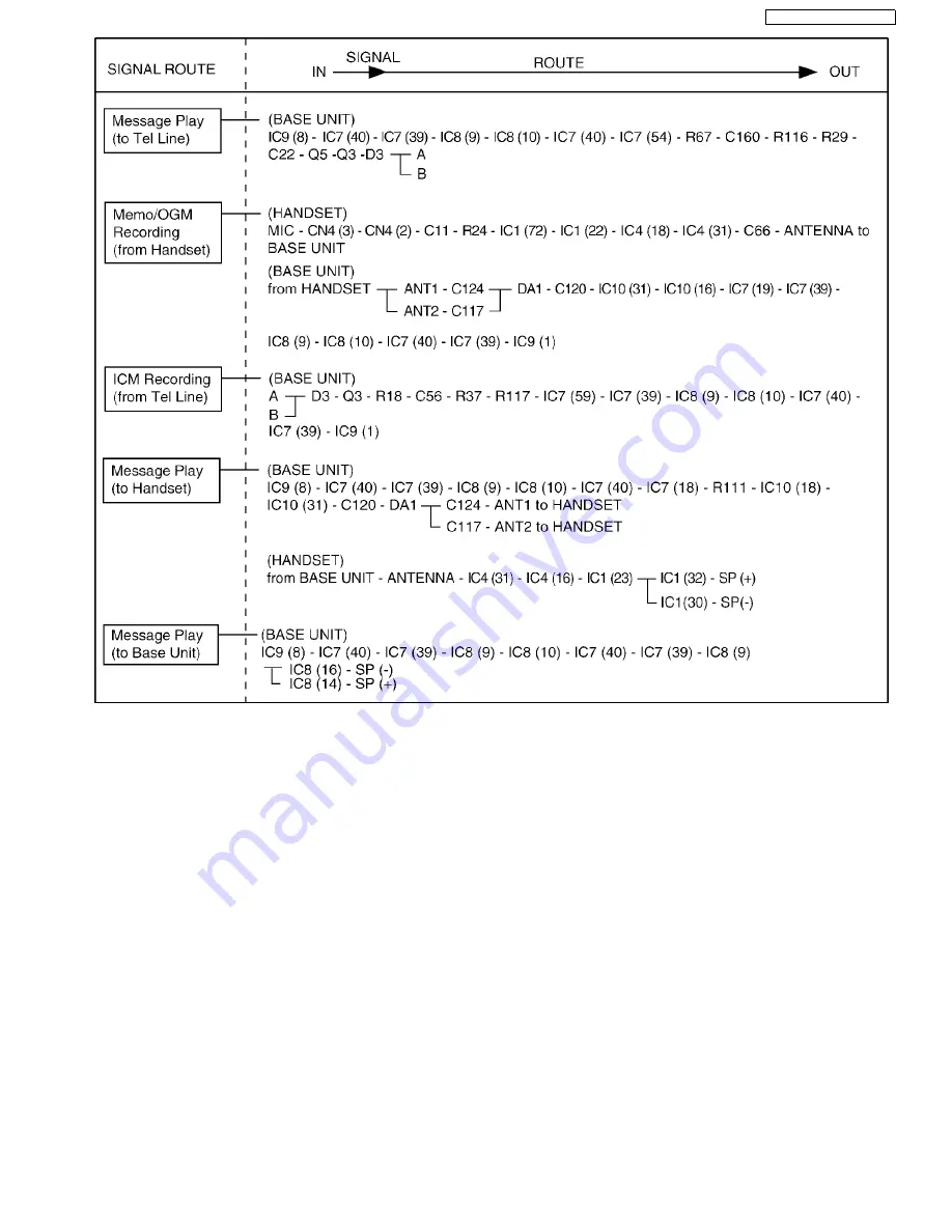
Page 10: ...ute P 14 4 2 4 1 Transmitter Block The voice signal input from the TEL LINE interface goes to RF Module IC10 through DECT BBIC IC7 as shown in Block Dia gram Base Unit P 7 The voice signal passes through the analog part of IC7 where it is amplified and converted to a digital audio stream signal The burst switch controller processes this stream performing encryption and scrambling adding the variou...

Page 11: ... SCL CPU Analog Front End D A A D 30 32 66 67 72 62 52 45 44 58 56 59 60 6 9 10 77 ADPCM Codec Filter DSP Speech Decoding Speech Encoding BMC Burst Decoding Burst Encoding RF Interface RF Module IC4 23 22 RXDA TXDA 19 26 25 24 RSSI SYDA SYEN SYCL 16 17 XTAL X1 10 368 MHz BATTERY 61 ON SWITCH KEYPAD ROWS COLUMNS 1 12 40 76 27 28 34 35 36 74 BBIC IC1 IC3 11 LCD BACK LIGHT Ringer LED 7 46 KX TGA101 B...

Page 12: ... 4 3 Charge Circuit Circuit Operation When charging the handset on the Base Unit the charge current is as follows DC 6 5 V R55 R56 CHARGE Base CHARGE Handset Q4 D7 F1 BATTERY Battery BATTERY R45 GND CHARGE Handset CHARGE Base GND DC GND In this way the BBIC on Handset detects the fact that the battery is charged The charge current is controlled by switching Q5 of Handset Refer to Fig 101 in Power ...

Page 13: ...13 KX TG1032SK KX TGA101S 4 5 Circuit Operation Charger Unit 4 5 1 Power Supply Circuit The power supply is as shown ...

Page 14: ...14 KX TG1032SK KX TGA101S 4 6 Signal Route ...

Page 15: ...15 KX TG1032SK KX TGA101S ...

Page 16: ...structions Instruction book on TSN Server 6 Installation Instructions Refer to the Operating Instructions Note You can download and refer to the Operating Instructions Instruction book on TSN Server 7 Operation Instructions Refer to the Operating Instructions Note You can download and refer to the Operating Instructions Instruction book on TSN Server ...

Page 17: ...17 KX TG1032SK KX TGA101S 8 Service Mode 8 1 Engineering Mode 8 1 1 Base Unit ...

Page 18: ...he table below Items Address Default Data New Data Remarks Frequency 00 01 75 Use these items in a READ ONLY mode to confirm the contents Careless rewriting may cause serious damage to the computer system ID 00 10 00 14 Given value Desired Number hex Input Keys Desired Number hex Input Keys 0 0 A Flash 0 1 1 B Flash 1 C Flash 2 D Flash 3 E Flash 4 9 9 F Flash 5 ...

Page 19: ...19 KX TG1032SK KX TGA101S 8 1 2 Handset ...

Page 20: ...irm the contents Careless rewriting may cause serious damage to the handset Items Address Default Data New Data Possible Adjusted Value MAX hex Possible Adjusted Value MIN hex Remarks Battery Low 00 04 25 2 Frequency 00 01 75 ID 00 10 00 14 Given value Desired Number hex Input Keys Desired Number hex Input Keys 0 0 A Flash 0 1 1 B Flash 1 C Flash 2 D Flash 3 E Flash 4 9 9 F Flash 5 ...

Page 21: ...which the customer has registered Refer to the following procedures Note BS Base Unit HS Handset If the max number of handsets are already registered to the base unit a new handset cannot be registered To register the handset refer to Registering a Handset P 34 To cancel the handset refer to Deregistering a handset P 34 To copy the handset phonebook refer to Copying Handset Phonebook Items P 34 ...

Page 22: ...dsets are already registered to the base unit a new handset cannot be registered To register the handset refer to Registering a Handset P 34 ToTo cancel the handset refer to Deregistering a handset P 34 ToTo copy the handset phonebook refer to Copying Handset Phonebook Items P 34 ...

Page 23: ...nit and handset Note 1 Refer to Registering a Handset P 34 Handset registration will not be reset 8 3 2 Resetting only handset The only handset is reset by doing the following steps to Note 2 The registration of the base unit and the handset are cancelled If the handset needs to be registered to the base unit refer to Registering a Handset P 34 If users do not bring the base unit with them the reg...

Page 24: ... 9 1 Troubleshooting Flowchart Cross Reference Check Power P 25 Bell Reception P 35 Check Battery Charge P 26 Check Link P 27 Check Handset Transmission P 35 Check Handset Reception P 35 Signal Route P 14 Check Caller ID P 35 Check TAM Operation P 36 ...

Page 25: ...1 Base Unit Is the AC Adaptor inserted into AC outlet 1 Cross Reference Power Supply Circuit P 9 Note 1 Refer to Specifications P 6 for part number and supply voltage of AC Adaptor 9 1 1 2 Handset Cross Reference Power Supply Circuit Reset Circuit P 12 ...

Page 26: ...KX TGA101S 9 1 2 Check Battery Charge 9 1 2 1 Base Unit Cross Reference Charge Circuit P 12 9 1 2 2 Handset Cross Reference Check Power P 25 Charge Circuit P 12 9 1 2 3 Charger Unit Cross Reference Charge Circuit P 12 ...

Page 27: ...27 KX TG1032SK KX TGA101S 9 1 3 Check Link 9 1 3 1 Base Unit Cross Reference Check Point Base Unit P 37 Power Supply Circuit P 9 Check the RF part P 29 ...

Page 28: ...28 KX TG1032SK KX TGA101S 9 1 3 2 Handset Cross Reference Check Point Handset P 37 Power Supply Circuit Reset Circuit P 12 Check the RF part P 29 ...

Page 29: ...F part 9 1 4 1 Finding out the Defective part After All the Checkings or Repairing 1 Re register the checked Handset to the checked Base Unit and Regular HS to Regular BU Note If you need to register a handset refer to Registering a Handset P 34 ...

Page 30: ...art Each item 1 6 of RF Check Flowchart corresponds to Check Table for RF part P 31 Please refer to the each item Note 1 Base unit refer to D of Check Point Base Unit P 37 Handset refer to F of Check Point Handset P 37 2 Refer to TEST RANGE Check P 32 ...

Page 31: ... X tal Frequency 4 10 368 MHz 100Hz 4 TX Power confirmation 5 HS BU mode Checked unit Burst TX mode 1 Regular unit Test RX mode 1 1 Place the Regular HS about 15cm away from the BU 2 Confirm that RSSI of the Regular HS is approximately 0 85 V by Oscilloscope 3 1 Place the HS about 15cm away from the Regular BU 2 Confirm that RSSI of the Regular BU is approximately 0 85 V by Oscilloscope 4 5 RX Sen...

Page 32: ...ng to CHART1 3 At distance of about 20m between HS and BU Link OK TX Power of the HS is OK No Link TX Power of the HS is NG Range Confirmation RX TEST RX sensitivity check HS BU setting Checked unit High TX power 1 Regular unit Low TX power 1 1 Register Regular HS to BU to be checked 2 Set TX Power of the BU and the Regular HS according to CHART1 3 At distance of about 20m between HS and BU Link O...

Page 33: ...33 KX TG1032SK KX TGA101S 9 1 4 5 RF BBIC Interface Signal Wave Form SYCL SYEN SYDA ...

Page 34: ...34 KX TG1032SK KX TGA101S 9 1 5 Registering a Handset 9 1 5 1 Deregistering a handset 9 1 6 Copying Handset Phonebook Items You can copy one or all of the phonebook items from one handset to another ...

Page 35: ...ception Cross Reference How to Check the Handset Speaker or Receiver P 55 Signal Route P 14 9 1 9 Check Caller ID Cross Reference Signal Route P 14 9 1 10 Bell Reception 9 1 10 1 Base Unit 9 1 10 2 Handset Cross Reference Telephone Line Interface P 10 Check Link P 27 How to Check the Handset Speaker or Receiver P 55 ...

Page 36: ...irst 2 seconds 2 If the Disable is selected even if the parallel connected telephone is OFF HOOK the line isn t disconnected B How to change the VOX level It makes easier to detect a small voice caller by raising the sensitivity of VOX level Therefore the recording of TAM is not turned off during a detection Cross Reference Power Supply Circuit P 9 Auto Disconnect detect PROCEDURE at Stand by mode...

Page 37: ...djustment 1 8 V 1 Confirm that the voltage between test point 1 8 V and GND is 1 8 V 0 02 V 2 Execute the command bandgap then check the current value 3 Adjust the 1 8V voltage of VDD1 executing command bandgap XX XX is the value IC1 Q2 C10 B DC DC Supply Confir mation 3 3 V 1 Confirm that the voltage between test point 3 3 V and GND is 3 3 V 0 3 V Backlight is ON IC1 F1 C1 C2 C3 R1 Q1 D1 L1 C 2 5...

Page 38: ...38 KX TG1032SK KX TGA101S 10 Disassembly and Assembly Instructions 10 1 Disassembly Instructions 10 1 1 Base Unit ...

Page 39: ...39 KX TG1032SK KX TGA101S ...

Page 40: ...40 KX TG1032SK KX TGA101S 10 1 2 Handset ...

Page 41: ...41 KX TG1032SK KX TGA101S 10 1 3 Charger Unit ...

Page 42: ...42 KX TG1032SK KX TGA101S ...

Page 43: ...43 KX TG1032SK KX TGA101S 10 2 How to Replace the Handset LCD ...

Page 44: ...44 KX TG1032SK KX TGA101S 10 3 How and Where to fix the spacer ...

Page 45: ...45 KX TG1032SK KX TGA101S ...

Page 46: ...ust like a mass production 11 2 The Setting Method of JIG Base Unit This section explains the PC setting to use command required in Check Point Base Unit P 37 Preparation Serial JIG cable PQZZ1CD300E PC which runs in DOS mode Batch file CD ROM for setting PQZZTG1032M Note If you have the JIG Cable for TCD500 series PQZZ1CD505E change the following values of resistance Then you can use it as a JIG ...

Page 47: ... ID RFPI Type readid and the registered ID is read out writeid Write ID RFPI Type writeid 00 18 E0 0E 98 and the ID 0018 E0 0E 98 is written setfreq Adjust Frequency of RFIC Type setfreq nn hookoff Off hook mode on Base Type hookoff hookon On hook mode on Base Type hookon getchk Read checksum Type getchk wreeprom Write the data of EEPROM Type wreeprom 01 23 45 01 23 is address and 45 is data to be...

Page 48: ... R34 R158 R32 R160 R13 R9 R7 R12 E E E E E R111 R151 R59 L6 JTAG L4 L5 L3 IC10 IC5 IC6 IC9 TP23 SA1 SA3 SA4 B SA2 D13 Q16 SW1 D14 D11 D7 D8 P1 J5 Q9 L2T TP RLY3 L1R TP RLY4 L1T TP RLY2 ANT 1 CN4 CN5 1 1 1 5 3 3 4 4 6 10 Q6 R48 US 1 TP RLY5 TP RLY1 C27 C2 C155 C20 C19 C18 C23 C24 C141 C29 C28 CN1 C117 C125 C51 C88 C91 C82 C83 C133 C81 C46 C62 C140 C153 C8 C7 C87 C129 C64 C31 C30 C32 CN2 C36 C37 C12...

Page 49: ...CHARGE CHARGE PQUP11502Z KX TG103 H RED SPEAKER PbF GND TX RX DC J104 J102 J103 J101 BLACK CHARGE 2 5V 3 3V 1 8V LINE DC RED BLACK A C84 C162 US 2 C56 C152 C74 C79 C78 C77 C72 C70 C69 C161 C68 C11 C57 C12 C58 C54 C55 C67 E E R115 R114 R80 R79 R78 R77 R162 R56 R76 R5 R6 R4 R3 R70 R69 R16 R36 R72 R15 R17 R21 R22 R19 R23 R75 R81 R86 R85 R84 1 1 16 17 32 33 48 49 64 5 3 4 L9 IC7 IC4 D9 D17 Q8 Q4 C48 C...

Page 50: ...11 4 Adjustment Standard Charger Unit When connecting the simulator equipment for checking please refer to below 11 4 1 Bottom View PQLV30053Z TP4 TP3 1 2 A PQUP11516Z PbF GND TP4 TP3 DC POWER 6 5 V Digital Volt Meter 12 2 W GND ...

Page 51: ...the JIG Cable for TCD500 series PQZZ1CD505E change the following values of resistance Then you can use it as a JIG Cable for both TCD300 and TCD500 series It is an upper compatible JIG Cable 11 5 1 Connections Connect the DC Power or Battery to BATT and BATT Handset Connect the JIG cable GND black Connect the JIG cable UTX yellow and URX red Note Com port names may vary depending on what your PC c...

Page 52: ...ddress 00 00 to FF is read out readid Read ID RFPI Type readid and the registered ID is read out writeid Write ID RFPI Type writeid 00 18 E0 0E 98 and the ID 0018 E0 0E 98 is written setfreq Adjust Frequency of RFIC Type setfreq nn getchk Read checksum Type getchk wreeprom Write the data of EEPROM Type wreeprom 01 23 45 01 23 is address and 45 is data to be written bursttx Burst TX mode Type burst...

Page 53: ... B 1 Current Probe Oscilloscope C91 UTX URX BATT C32 C92 C15 L3 L1 L75 L72 L71 L14 L6 C97 C148 C150 R12 GND BAT R11 R33 R47 R61 R32 MIC MIC CHG CHG MIC D8 C147 C137 C138 C152 C71 C70 C52 C53 C51 C86 C128 C127 CLK 1 27 26 17 16 32 10 11 CLK_G ANT_G C57 C58 C62 C61 C59 C60 C101 C3 C39 C22 C26 JTAG POWER RA1 RECEIVER R53 R52 R143 R201 R96 R43 R7 R202 3 3V 2 5V E 1 8V F1 BATT R125 Q8 E Q1 Q10 Q9 Q4 E ...

Page 54: ...splayed on the PC indicating downloading has finished 6 Detach the JIG cable then disconnect the DC Power 7 Connect the DC Power 8 Connect the JIG cable again and execute the command getchk then confirm the checksum value is correct If the downloading fails start again from step 1 EEPROM IC5 Adjustment parameter data country version batch file default batch file etc 1 Clock adjustment Refer to Che...

Page 55: ...s shown below 11 9 Frequency Table MHz Note Channel No 2 In the Test Mode on Base Unit and Handset BASE UNIT HANDSET Channel No Transmit Frequency Receive Frequency Transmit Frequency Receive Frequency 0 1928 448 1928 448 1928 448 1928 448 1 1926 720 1926 720 1926 720 1926 720 2 1924 992 1924 992 1924 992 1924 992 3 1923 264 1923 264 1923 264 1923 264 4 1921 536 1921 536 1921 536 1921 536 ...

Page 56: ...damage the PCB foil Flux Recommended Flux Specific Gravity 0 82 Type RMA lower residue non cleaning type Note See About Lead Free Solder Pbf Pb free P 4 12 1 2 How to Remove the IC 1 Put plenty of solder on the IC pins so that the pins can be completely covered Note If the IC pins are not soldered enough you may give pressure to the P C board when cutting the pins with a cutter 2 Make a few cuts i...

Page 57: ...he IC setting with the corresponding soldering foil 2 Apply flux to all pins of the FLAT PACKAGE IC 3 Solder the pins sliding the soldering iron in the direction of the arrow 12 1 4 How to Remove a Solder Bridge 1 Lightly resolder the bridged portion 2 Remove the remaining solder along the pins using a soldering iron as shown in the figure below ...

Page 58: ...fficiently choose the right sized nozzle of the hot air desoldering tool that matches the IC package Be careful about the temperature of the hot air desoldering tool not to damage the PCB and or IC 12 2 3 How to Remove the IC 1 Heat the IC with a hot air desoldering tool through the P C board 2 Pick up the IC with tweezers etc when the solder is melted completely Note Be careful not to touch the p...

Page 59: ... the positioning should be done very carefully 3 Heat the IC with a hot air desoldering tool through the P C board until the solder on IC bottom is melted Note Be sure to place it precisely controlling the air volume of the hot air desoldering tool 4 After soldering confirm there are no short and open circuits with visual inspection 12 2 5 How to Remove a Solder Bridge When a Solder Bridge is foun...

Page 60: ...60 KX TG1032SK KX TGA101S 12 3 Terminal Guide of the ICs Transistors and Diodes 12 3 1 Base Unit 12 3 2 Handset ...

Page 61: ...velopment of new technology 13 1 2 Handset Schematic Diagram Handset Notes 1 DC voltage measurements are taken with an oscilloscope or a tester with a ground 2 The schematic diagram may be modified at any time with the development of new technology 13 1 3 Charger Unit Schematic Diagram Charger Unit Notes 1 DC voltage measurements are taken with voltmeter from the negative voltage line 2 The schema...

Page 62: ...m 16 VDDRF 17 RFCLKd 18 TDO 19 RDI 20 SK 21 PD1 SIO 22 LE 23 P31 PD1 24 P32 PD2 25 P33 PD3 26 P34 PD4 27 TDOD P35 PD5 28 P36 PD6 29 VSS2 30 VDDIO2 31 VDD2 32 PCM_FSC INT0 P10 33 P00 UTX 34 P01 URX 35 P02 JTIO 36 P03 SDA2 37 P04 SCL2 38 P05 SPICLK PCM_CLK 39 P06 SPIDO PCM_DOUT 40 P07 SPIDI PCM_DIN 41 VSS3 42 VDD3 43 P23 ADC1 44 P17 CHARGE INT7 45 RST 46 VBAT1 47 LDO1_CTRL 48 LDO2_CTRL 49 LDO1_Sense...

Page 63: ...NC C115 NC C131 NC 150p C126 1 GND1 2 ANT2 3 VCCPA 4 GND2 5 GND3 6 VCC_OC 7 GND4 8 RSSI 9 SYRI 10 GND5 11 GND6 12 SYEN 13 SYDA 14 SYCL 15 GND7 16 RX_DATA 17 GND8 18 TXDA 19 GND9 20 RESET 21 ANT1 22 GND10 23 GND11 24 GND12 25 GND13 26 GND14 27 GND15 28 GND16 29 GND17 30 GND18 31 A_1 32 GND19 1u C84 R156 NC GND 3 C122 NC D10p C125 D10p C118 0 L11 2 2n C120 L7 15n C117 10p 1n L10 L3 C0 5p 180 R106 D1...

Page 64: ...C STOP 1 2 ERASE 1 2 LOCATOR 1 2 GND VDD LED2T ANS_ON 1 2 CN10 1 CN10 2 CN10 6 ROW0 CN10 7 LED1 CN10 8 VDD CN10 9 LED2 CN10 10 KEY1 CN10 4 ROW2 CN10 3 ROW1 CN10 5 KEY0 SKIP 1 2 REPEAT 1 2 VOL_UP 1 2 VOL_DOWN 1 2 PLAY 1 2 LED1T PLAY LED1 1 2 KX TG1032 SCHEMATIC DIAGRAM Base Unit_Operation ...

Page 65: ...65 KX TG1032SK KX TGA101S Memo ...

Page 66: ...VSS2 39 VDD2 41 P00 UTX 43 P02 JTIO 45 P04 SCL2 47 P06 SPIDO PCM_DOUT 49 VSS3 51 P23 ADC1 53 RST 55 DC_I 57 DC_Sense 100n C25 C94 NC 5 6k R46 220k R7 10k R64 5 6k R47 BATTERY 470 R23 3 3k R24 LED10 A K Q9 120 R92 C5 2 2u C10 2 2u UP 1 2 DOWN 1 2 RIGHT 1 2 LEFT 1 2 0 1 2 1 1 2 2 1 2 3 1 2 4 1 2 5 1 2 6 1 2 7 1 2 8 1 2 TALK 1 2 S1 1 2 1k R66 C93 NC 9 1 2 SOFT_C 1 2 SOFT_B 1 2 SHARP 1 2 AST 1 2 SOFT_...

Page 67: ...2 K1000p C58 K1000p C108 NC C82 K470p 100n C156 C152 NC C37 NC NC C110 C140 NC 150p C53 39p C57 1 GND1 2 ANT2 3 VCCPA 4 GND2 5 GND3 6 VCC_OC 7 GND4 8 RSSI 9 SYRI 10 GND5 11 GND6 12 SYEN 13 SYDA 14 SYCL 15 GND7 16 RX_DATA 17 GND8 18 TXDA 19 GND9 20 RESET 21 ANT1 22 GND10 23 GND11 24 GND12 25 GND13 26 GND14 27 GND15 28 GND16 29 GND17 30 GND18 31 A_1 32 GND19 NC L75 0 R201 R202 NC C33 NC L71 L72 1 5k...

Page 68: ...68 KX TG1032SK KX TGA101S 13 5 Schematic Diagram Charger Unit TP4 G 12 R2 TP3 12 R4 J1 2 1 10 R1 10 R3 TP1 TP2 SCHEMATIC DIAGRAM Charger Unit ...

Page 69: ...R13 R9 R7 R12 E E E E E R111 R151 R59 L6 JTAG L4 L5 L3 IC10 IC5 IC6 IC9 TP23 SA1 SA3 SA4 SA2 D13 Q16 SW1 D14 D11 D7 D8 P1 J5 Q9 L2T TP RLY3 L1R TP RLY4 L1T TP RLY2 ANT 1 CN4 CN5 1 1 1 5 3 3 4 4 6 10 Q6 R48 US 1 TP RLY5 TP RLY1 C27 C2 C155 C20 C19 C18 C23 C24 C141 C29 C28 CN1 C117 C125 C51 C88 C91 C82 C83 C133 C81 C46 C62 C140 C153 C8 C7 C87 C129 C64 C31 C30 C32 CN2 C36 C37 C122 C124 C111 C112 C102...

Page 70: ...62 R56 R76 R5 R6 R4 R3 R70 R69 R16 R36 R72 R15 R17 R21 R22 R19 R23 R75 R81 R86 R85 R84 1 1 16 17 32 33 48 49 64 5 3 4 L9 IC7 IC4 D9 D17 Q8 Q4 C48 C17 C76 BUZ C15 C14 C13 C16 C25 C49 C149 C151 C47 C143 C134 C148 C150 C86 C154 C75 C144 C139 C138 C65 C61 C73 C136 C137 C6 L1T L2T DCM VDD1 VDD2 A 1 CLK SP SP A 2 VDD3 ANT L2R L1R 1 1 3 2 2 4 C5 C60 C59 C66 C1 R55 R27 R28 R74 R161 R1 R88 R87 R68 R117 R66...

Page 71: ...Circuit Board Base Unit_Operation 14 2 1 Bottom View KX TG103 H REPEAT ERASE LOCATOR 1 10 PQUP11503Z VOL_DOWN VOL_UP A STOP PLAY CN10 SKIP ANS_ON LED2 LED1 GND LED1 LED2 VDD PbF KX TG1032 CIRCUIT BOARD Base Unit_Operation Bottom View ...

Page 72: ...72 KX TG1032SK KX TGA101S Memo ...

Page 73: ...V F1 BATT R125 Q8 E Q1 Q10 Q9 Q4 E D1 C55 D19 RED BLACK RED BLACK D20 C50 C90 C49 C48 C42 C54 C56 C140 C72 C38 CN4 C2 C1 C110 C108 C83 4 3 2 5 1 C82 C113 C35 C151 C157 C5 C18 C17 C21 C73 C33 C8 C37 C156 C10 C24 C19 1 20 21 40 41 60 61 80 C149 C20 C7 C6 C25 C14 C93 C94 C109 C107 C34 C36 C11 C12 C30 C96 R25 R45 R5 R8 R89 R93 R90 R92 R54 R2 R1 R51 ANT R6 R46 R14 R42 D13 SPEAKER R41 R40 R66 R63 R44 R1...

Page 74: ... 18 1 R140 R141 C40 R95 R94 C43 C44 C45 C46 C47 C143 C144 C142 C141 C41 R142 PQUP11501Z LEFT TALK SP 1 2 3 4 5 6 7 8 9 INT R C MIC MIC MIC 0 UP DOWN SOFT_B SOFT_C SOFT_A CANCEL S1 RIGHT LED3 LED2 LED1 LED10 KX TGA101 CIRCUIT BOARD Handset Bottom View ...

Page 75: ...ircuit Board Charger Unit 14 4 1 Component View 14 4 2 Bottom View PQLV30053Z R3 R4 R1 J1 A R2 1 2 PQUP11516Z PbF CIRCUIT BOARD Charger Unit Component View PQLV30053Z TP4 TP3 1 2 A PQUP11516Z PbF CIRCUIT BOARD Charger Unit Bottom View ...

Page 76: ...76 KX TG1032SK KX TGA101S 15 Exploded View and Replacement Parts List 15 1 Cabinet and Electric Parts Base Unit ...

Page 77: ...c Parts Handset Note 1 This cable is fixed by welding Refer to How to Replace the Handset LCD P 43 2 The rechargeable Ni MH battery HHR 4DPA is available through sales route of Panasonic 3 Attach the spacer No 122 to the exact location described above ...

Page 78: ...78 KX TG1032SK KX TGA101S 15 3 Cabinet and Electric Parts Charger Unit ...

Page 79: ...79 KX TG1032SK KX TGA101S 15 4 Accessories ...

Page 80: ...SPEAKER 4 PQHG10729Z RUBBER PARTS SPEAKER 5 PQHR10778Z GUIDE SPEAKER ABS HB 6 PQJT10241V CHARGE TERMINAL L 7 PQJT10242X CHARGE TERMINAL R 8 PQKE10454Z1 HOLDER CHARGE TERMI NAL L POM HB 9 PQKE10455Z1 HOLDER CHARGE TERMI NAL R POM HB 10 PQKE10474Y1 CASE CHARGE TERMINAL PS HB 11 PQBC10497Z1 BUTTON MESSAGE AS HB 12 PQSX10343Z KEYBOARDSWITCH RUBBER 13 PQKF10739Y1 CABINET COVER PS HB 14 PQHA10023Z RUBBE...

Page 81: ...V 0 068 C25 ECUV1C104KBV 0 1 C27 F2G1H1000009 10 Safety Ref No Part No Part Name Description Remarks C30 ECUV1C104KBV 0 1 C32 ECEA1CK101 100 S C36 ECEA0JKA331 330 C37 ECUV1C104KBV 0 1 C48 ECUV1H103KBV 0 01 C50 ECUE1C103KBQ 0 01 C51 ECUE1A104KBQ 0 1 C52 ECUV1H221JCV 220p C53 ECUV1H221JCV 220p C54 ECUE1C223KBQ 0 022 C55 ECUE1A104KBQ 0 1 C56 ECUV1C104KBV 0 1 C59 ECUE1A104KBQ 0 1 C60 ECUE1A104KBQ 0 1 ...

Page 82: ...STOR SI Q3 B1ADGE000004 TRANSISTOR SI Q4 B1ADGE000004 TRANSISTOR SI Q5 B1ABCF000103 TRANSISTOR SI S Q8 UN9219J TRANSISTOR SI S Q9 UN9219J TRANSISTOR SI S DIODES D1 B0JCME000035 DIODE SI D7 MA2Z72000 DIODE SI D19 MA8047 DIODE SI S D20 MA8047 DIODE SI S LEDS LED1 B3ACB0000139 LED LED2 B3ACB0000139 LED LED3 B3ACB0000139 LED LED10 B3ACB0000134 LED IC FILTERS L3 J0JCC0000287 IC FILTER L6 J0JCC0000275 I...

Page 83: ...C104KBV 0 1 C150 ECUE1A104KBQ 0 1 C151 ECUE1A104KBQ 0 1 C156 ECUV1C104KBV 0 1 OTHERS MIC L0CBAY000018 MICROPHONE E101 L5DCAYY00010 LIQUID CRYSTAL DISPLAY 2 E102 PQHX11378Z COVER LCD E103 PQHR11195Z TRANSPARENTPLATE LCD PMMA HB E104 PQHR11205Z GUIDE LCD ABS HB IC4 PQLP10291Z RF UNIT CN4 K2HD103D0001 JACK D8 D4ED1270A014 VARISTOR SURGE ABSORBER X1 H0J103500021 CRYSTALOSCILLATOR 1 Safety Ref No Part ...

Reviews: