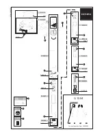
background image

S-4

S4. Schematic Diagram

S4.1. Interconnection Diagram

HDC-HS20,HS25

INTERCONNECTION DIAGRAM

SUB P.C.B.

(FOIL SIDE)

SIDE (R) P.C.B.

(FOIL SIDE)

MONITOR P.C.B.

(FOIL SIDE)

FRONT P.C.B. (FOIL SIDE)

MAIN P.C.B.

(FOIL SIDE)

MONITOR

FPC_B

SPEAKER

LCD UNIT

MOS

UINT

LENS

UNIT

MOS FPC

BATTERY

POWER FPC

MIC

ECM FPC

FRONT CASE UNIT

(LENS BARRIER)

FP6501

PS6102

90

D_GND

89

D_GND

88

D_GND

87

D_GND

86

D_GND

85

D_GND

84

D_GND

83

D_GND

82

D_GND

81

D_GND

80

D_GND

79

D_GND

78

D_GND

77

S_HDD_G_SCL

76

S_HDD_G_SDA

75

PW_REG8R5V

74

PW_REG5V

73

VREF_BOSS

72

E_POW_RST

71

P_ON_H

70

PW_HDD3R3V

69

PW_HDD3R3V

68

PW_HDD3R3V

67

PW_REG3V

66

PW_REG3V

65

PW_REG3V

64

HDD_CONT

63

MOSSENSOR_ON

62

PW_NOREG

61

PW_MOS2R3V

60

PW_MOS2R3V

59

PW_MOS2R3V

58

SW_NOREG

57

PW_SWNOREG2

56

PW_SWNOREG2

55

PW_HDM5V

54

PW_VBUS

53

VBUS_CURED_L

52

VBUS_ON_H

51

BATT_T

50

E_S_BATT_TXD

49

S_BATT_RXD

48

D_GND

47

USB_D+

46

USB_D-

P6102

FP6503

FP6502

FP902

P6501

2T

R

IG

1

D

_GND

1 SP2

2 SP1

1 PW_LCD3R2V

2 PW_LCD3R2V

3 BUS9_PNLD7

4 BUS9_PNLD6

5 BUS9_PNLD5

6 BUS9_PNLD4

7 BUS9_PNLD3

8 BUS9_PNLD2

9 BUS9_PNLD1

10 BUS9_PNLD0

11 CLK18_PNL

12 BUS9_PNL_V

13 BUS9_PNL_H

14 LCDPNL_CS

15 S_DAT_LCDPNL

16 S_CLK_LCDPNL

17 PW_LCD1R8V

18 PW_LCD1R8V

FP901

1 PW_MBL5V

2 PW_MBL5V

3 PW_REG3V

4 D_GND

5 D_GND

6 D_GND

7 D_GND

8 D_GND

9 S_CLK_TPNL

10 TPNL_CS

11 S_S2T_TPNL

12 S_T2S_TPNL

13 BL_CONT

14 KEYIN6

FP6400

FP905 1

KEYIN6

2

KEYIN6

3

D

_GND

4

D

_GND

FP904

10

LENSBA_MT_B-

9

LENSBA_MT_A-

8

LENS

7

LENS

6N

C

5

OP_SHTER_LED

4N

C

3

D_GND

2N

C

1

S

HTR_OPEN

FP4801

6

ECM[L]

5

GND

4

ECM[B]

3

GND

2

GND

1

ECM[R]

MONITOR

FPC_A

TOP/ OPERATION UNIT

FRONT

FPC

MAIN

SUB FPC

FLASH

UNIT

FP903

4

XP

3

YN

2

XN

1

YP

TOUCH PANEL

LCD OP FPC (FOIL SIDE)

(COMPONENT SIDE)

FP6403

32

TALLY_LED_B

30

S_REMO_R2R

28

PW_REG3V

26

G_GYROY

24

G_GYROP

22

D_GND

20

MIC_GND

18

G_MIC_OUT_R

16

GND[MICOUTC]

14

G_MIC_OUT_L

12

PW_REG5V

10

LENSBA_MT_A-

8

LENS

6

LENSBA_MT_B-

4

LENS

2

O

P_SHTER_LED

33

NC[TALLY_LED_B]

31

PW_LI_BATT

29

PW_REMO_3V

27

G_GYRO_REFY

25

G_GYRO_REFP

23

GYRO_GND

21

D_GND

19

MIC_GND

17

G_MIC_OUT_B

15

GND[MICOUTF]

13

PW_REG5V

11

LENSBA_MT_A-

9

LENS

7

LENSBA_MT_B-

5

LENS

3

SHTER_OPEN

1

LIGHT_ON_H

16 D_GND

14 BL_CONT

12 S_S2T_TPNL

10 S_CLK_TPNL

8 D GND

6 D_GND

4 PW_REG3V

2 PW_MBL5V

17 LCD_RVS

15 KEYIN6

13 S_T2S_TPNL

11 TPNL_CS

9 D_GND

7 D_GND

5 D_GND

3 PW_REG3V

1 PW_MBL5V

16 LCDPNL_CS

14 S_CLK_LCDPNL

12 BUS9_PNL_V

10 BUS9_PNLD0

8 BUS9_PNLD2

6 BUS9_PNLD4

4 BUS9_PNLD6

2 PW_LCD3R2V

17 PW_LCD1R8V

15 S_DAT_LCDPNL

13 BUS9_PNL_H

11 CLK18_PNL

9 BUS9_PNLD1

7 BUS9_PNLD3

5 BUS9_PNLD5

3 BUS9_PNLD7

1 PW_LCD3R2V

40 KEYIN5

38 PW_REG3V

36 PW_MBL5V

34 S_CLK_TPNL

32 S_S2T_TPNL

30 SPOUT2/PW_FAN5V

28 SPOUT1/FAN_FG

26 D_GND

24 D_GND

22 D_GND

20 D_GND

18 D_GND

16 BUS13_SLLCD0

14 BUS13_SLLCD2

12 BUS13_SLLCD4

10 BUS13_SLLCD6

8 PW_LCD1R8V

6 CLK27_SLLCD

4 PW_LCD3R2V

2 S_DAT_LCDPNL

41 NC

39 KEYIN6

37 PW_MBL5V

35 LCD_RVS

33 TPNL_CS

31 S_T2S_TPNL

29 SPOUT2/PW_FAN5V

27 SPOUT1/FAN_FG

25 D_GND

23 D_GND

21 D_GND

19 D_GND

17 D_GND

15 BUS13_SLLCD1

13 BUS13_SLLCD3

11 BUS13_SLLCD5

9 BUS13_SLLCD7

7 PW_LCD1R8V

5 PW_LCD3R2V

3 S_CLK_LCDPNL

1 LCDPNL_CS

36 VCS

34 VGL

32 CP9

30 CP7

28 CP5

26 CP3

24 CP1

22 GNDA

20 GND

18 VDD

16 VCC

14 DIN6

12 DIN4

10 DIN2

8 DIN0

6 VSYNC

4 SCL

2 CSB

37 VCOM

35 VGH

33 CP10

31 CP8

29 CP6

27 CP4

25 CP2

23 VDDA

21 GNDA

19 VDD

17 VDDIO

15 DIN7

13 DIN5

11 DIN3

9

DIN1

7

DCLK

5

HSYNC

3

SDA

1

STB

1

CLK12_SDCMD

2

PROTECT

3

BUS12_SDDAT0

4

BUS12_SDDAT1

5

BUS12_SDDAT2

6

BUS12_SDDAT3

7

E_CARD_DET

8

CLK24_SDCARD

9

PW_UNI1R2V

10

PW_UNI1R2V

11

PW_UNI1R2V

12

PW_UNI1R2V

13

PW_UNI1R2V

14

PW_UNI1R2V

15

TRIGEND

16

CHAEND

17

CHARGE

18

SPOUT1

19

SPOUT2

20

DOOR_OPEN

21

CARD_LED_B

22

PW_LI_BATT

23

E_HDD_G_RES

24

G_HDD_G_INT

25

PW_3R2V

26

PW_3R2V

27

PW_3R2V

28

PW_MOS_-1V

29

PW_REG1R8V

30

PW_REG1R8V

31

PW_REG1R8V

32

PW_REG1R8V

33

PW_REG1R8V

34

PW_5V

35

PW_5V

36

PW_5V

37

PW_REG1R0V

38

PW_REG1R0V

39

PW_REG1R0V

40

PW_REG1R0V

41

PW_REG1R0V

42

PW_REG1R0V

43

USB_IDDET_L

44

D_GND

45

D_GND

PS6101 12

SPOUT2

11

SPOUT1

10

BATT_+

9

BATT_+

8

BATT_+

7

BATT_+

6T 5D 4

BATT_-

3

BATT_-

2

BATT_-

1

BATT_-

13

SPOUT2

14

SPOUT1

15

BATT_+

16

BATT_+

17

BATT_+

18

BATT_+

19

BATT_+

20

BATT_-

21

BATT_-

22

BATT_-

23

BATT_-

24

BATT_-

FP6003

2 LIGHT_ON_H

4 SHTER_OPEN

6 LENS

8 LENSBA_MT_B-

10 LENS

12 LENSBA_MT_A-

14 PW_5V

16 D_GND(MIC_F)

18 G_MIC_OUT_B

20 MIC_GND

22 D_GND

24 GYRO_GND

26 G_GYRO_REFP

28 G_GYRO_REFY

30 PW_REMO_3V

32 LI_BATT

1 LIGHT_ON_H

3 OP_SHTER_LED

5 LENS

7 LENSBA_MT_B-

9 LENS

11 LENSBA_MT_A-

13 PW_5V

15 G_MIC_OUT_L

17 D_GNDMIC_C

19 G_MIC_OUT_R

21 MIC_GND

23 D_GND

25 G_GYROP

27 G_GYROY

29 PW_REG3VLB

31 S_REMO_R2R

33 TALLY_LED_B

FP6002

2

ZABS

4

IRHIN+

6

IRHIN-

8I

RM

+

10

FLEDCONT

12

FENCVCC

14

FBN

16

FBP

18

20

YAWHIN-

22

24

26

PITHIN-

28

30

ZBN

32

ZBP

1

ZLEDCONT

3

ZENCVCC

5

IRHO+

7I

RH

O

-

9I

RM

-

11

FABS

13

LENS_TEMP

15

FAN

17

FAP

19

YAWDRV-

21

YAWHO+

23

YAWHO-

25

PITHO-

27

PITHO+

29

PITDRV-

31

ZAP

33

ZAN

FP6006

1

AVREF(ZOOM)

3

ZOOMAD

5D

_G

ND

7N

C

9

E_KEYIN3

11

E_KEYIN1

13

STANDBY_LED

15

NC

2N

C

4N

C

6N

C

8

AVREF

10

POWER_SW

12

POWER_LED

14

DISK_LED

16

D_GND(LED)

P6101 1

XEON+

2

XEON+

(COMPONENT SIDE)

SIDE (R) FPC

PS6004

1 2 3 4 5 6 7 8 9 10 11 12 13 14 15 16 17 18 19 20 21 22 23 24 25 26 27 28 29 30 31 32 33 34 35 36 37 38 39 40 41 42 43 44 45

46 47 48 49 50 51 52 53 54 55 56 57 58 59 60 61 62 63 64 65 66 67 68 69 70 71 72 73 74 75 76 77 78 79 80 81 82 83 84 85 86 87 88 89 90

D_GND D_GND D_GND D_GND D_GND D_GND D_GND D_GND D_GND D_GND D_GND D_GND D_GND S_HDD_G_SCL S_HDD_G_SDA PW_REG8R5V W_REG5V VREF_BOSS E_POW_RST P_ON_H PW_HDD3R3V PW_HDD3R3V PW_HDD3R3V PW_REG3V PW_REG3V PW_REG3V HDD_CONT MOSSENSOR_ON PW_NOREG PW_MOS2R3V PW_MOS2R3V PW_MOS2R3V SW_NOREG PW_SWNOREG2 PW_SWNOREG2 PW_HDM5V VBUS VBUS_CURDE_L VBUS_ON_H E_BATT_T S_BATT_TXD S_BATT_RXD D_GND USB_D+ USB_D-

BUS12_SDCMD PROTECT BUS12_SDDAT0 BUS12_SDDAT1 BUS12_SDDAT2 US12_SDDAT3 CARD_DET CLK24_SDCARD PW_UNI1R2V PW_UNI1R2V PW_UNI1R2V PW_UNI1R2V PW_UNI1R2V PW_UNI1R2V TRIGEND CHAEND CHARGE SPOUT

[1]

SPOUT

[2]

DOOR_OPEN CARD_LED_B PW_LI_BATT E_HDD_G_RES G_HDD_G_INT PW_3R2V PW_3R2V PW_3R2V PW_MOS-1V PW_REG1R8V PW_REG1R8V PW_REG1R8V PW_REG1R8V PW_REG1R8V PW_5V PW_5V PW_5V PW_REG1R0V PW_REG1R0V PW_REG1R0V PW_REG1R0V PW_REG1R0V PW_REG1R0V USB_IDDET_L D_GND D_GND

PP6003

PS6001

20 19 18 17 16 15 14 13 12 11 10 9 8 7 6 5 4 3 2 1

21 22 23 24 25 26 27 28 29 30 31 32 33 34 35 36 37 38 39 40

PW_REG3V PW_MBL5V PW_MBL5V KEYIN6 KEYIN5 D_GND SPOUT2/PW_F

AN5V

SPOUT1/F

AN_FG

D_GND D_GND D_GND D_GND D_GND D_GND D_GND LCDPNL_CS S_D

AT_LCDPNL

S_CLK_LCDPNL PW_LCD3R2V PW_LCD3R2V

LCD_RVS S_CLK_TPNL TPNL_CS S_S2T_TPNL S_T2S_TPNL SPOUT2/PW_FAN5V SPOUT1/FAN_FG D_GND D_GND D_GND BUSI3_SLLCD0 BUSI3_SLLCD1 BUSI3_SLLCD2 BUSI3_SLLCD3 BUSI3_SLLCD4 BUSI3_SLLCD5 BUSI3_SLLCD6 BUSI3_SLLCD7 PW_LCD1R8V CLK27_SLLCD

1 2 3 4 5 6 7 8 9 10 11 12 13 14 15 16 17 18 19 20

40 39 38 37 36 35 34 33 32 31 30 29 28 27 26 25 24 23 22 21

HDD3R3V DASP CS0 DA0 INTRQ INTRQ HDD_GND DIOW DMARQ ATADATA15 ATADATA14 ATADATA13 ATADATA12 ATADATA11 ATADATA10 ATADATA9 ATADATA8 HDD_GND TEMP_GND TEMP_OUT

HDD3R3V HDD_UNLOAD CS1 DA2 DA1 DMACK IORDY DIOR HDD_GND HDD_GND ATADATA0 ATADATA1 ATADATA2 ATADATA3 ATADATA4 ATADATA5 ATADATA6 ATADATA7 RESET TEMP_VCC

FP6001

26 24 22 20 18 16 14 12 10 8 6 4 2

27 25 23 21 19 17 15 13 11 9 7 5 3 1

G_CMOS_OUT3 G_CMOS_OUT1 VSSA PW_3R3V SIGRS H1 PW_1R2V PW_4R1V VSS E_RSTN SCLK VSSA G_CMOS_OUT2 G_CMOS_OUT4

VSSA VSSA PW_AFE3R3V PW_3R3V H2 PW_-0R95V PW_2V VSS S_VST SDATA CSN VSSA VSSA

FTP6801 4D

_G

N

D

3D

_G

N

D

2

K

EYIN6

1

K

EYIN6

HDD UNIT

Summary of Contents for HDC-HS20P

Page 1: ...ation of law ORDER NO VM0901011CE B27 High Definition Video Camera Model No HDC HS20P HDC HS20PU HDC HS20EG HDC HS20EE HDC HS20EB HDC HS20EC HDC HS20EP HDC HS20GC HDC HS20GK HDC HS20EF HDC HS20GJ HDC HS20GN HDC HS20GT HDC HS20PC HDC HS20SG HDC HS25EB VOL 1 Colours K Black Type ...

Page 2: ...ing HDD 11 3 4 Formatting HDD 15 4 Specifications 16 5 Location of Controls and Components 17 6 Service Mode 22 6 1 Service Menu 22 6 2 About Default Setting 27 7 Service Fixture Tools 28 7 1 Service Tools and Equipment 28 8 Disassembly and Assembly Instructions 29 8 1 Disassembly Flow Chart 29 8 2 P C B Layout 29 8 3 Disassembly Procedures 30 8 4 Disassembly Procedures of Camera Lens Unit 41 9 Me...

Page 3: ... the customer from being exposed to shock hazards 1 1 1 Leakage Current Cold Check 1 Unplug the AC cord and connect a jumper between the two prongs on the plug 2 Measure the resistance value with an ohmmeter between the jumpered AC plug and each exposed metallic cabinet part on the equipment such as screwheads connectors control shafts etc When the exposed metallic part has a return path to the ch...

Page 4: ...f the assembly 3 Use only a grounded tip soldering iron to solder or unsolder ES devices 4 Use only an antistatic solder removal device Some solder removal devices not classified as antistatic ESD protected can generate electrical charge sufficient to damage ES devices 5 Do not use freon propelled chemicals These can generate electrical charges sufficient to damage ES devices 6 Do not remove a rep...

Page 5: ...s used Definition The letter of PbF is printed on the PCB using the lead free solder To put lead free solder it should be well molten and mixed with the original lead free solder Remove the remaining lead free solder on the PCB cleanly for soldering of the new IC Since the melting point of the lead free solder is higher than that of the normal lead solder it takes the longer time to melt the lead ...

Page 6: ...g must not be used until a replacement cover is obtained A replacement fuse cover can be purchased from your local Panasonic Dealer If the fitted moulded plug is unsuitable for the socket outlet in your home then the fuse should be removed and the plug cut off and disposed of safety There is a danger of severe electrical shock if the cut off plug is inserted into any 13 ampere socket If a new plug...

Page 7: ...ic It must never be subjected to excessive heat or discharge It must therefore only be fitted in equipment designed specifically for its use Replacement batteries must be of the same type and manufacture They must be fitted in the same manner and location as the original battery with the correct polarity contacts observed Do not attempt to re charge the old battery or re use it for any other purpo...

Page 8: ...8 2 5 How to Recycle the Lithium Battery U S Only ...

Page 9: ...Adapter used on the following model HDC HS20GK However the AC Adapter replacement part number is DE A51DA which should be used when ordering 4 VSK700 is indicated on AC Adapter used on the following models HDC HS20GT However the AC Adapter replacement part number is DE A51EA which should be used when ordering Notes 2 1 This service manual does not contain the following information because of the i...

Page 10: ...10 3 2 Service Caution 3 2 1 How to Discharge the Capacitor on the Sub P C B Remove the Sub P C B Refer to Disassembly Procedures ...

Page 11: ...Handle HDD very carefully to prevent the static electricity and shock 2 Set the HDD quickly after taking it out from the package Make sure to put the HDD on buffer materials etc 3 3 1 Precautions at incoming process and for opening packages ...

Page 12: ...12 3 3 2 Precautions for installing HDD ...

Page 13: ...or inserting and removing HDD FPC Make sure to use the tool LSVQ0112 when locking and unlocking the lock lever of HDD FPC connector Do not lock the lock lever without inserting HDD FPC Otherwise the connector may be damaged ...

Page 14: ...14 Make sure to use the tool LSVQ0112 when opening and closing the lock lever See Disassembly and Assembly Instructions Fig D10 for attaching to the unit ...

Page 15: ...15 3 4 Formatting HDD ...

Page 16: ...16 4 Specifications ...

Page 17: ...17 5 Location of Controls and Components Followings are the Location of Controls and Components for HDC TM20P PC as a sample For other models refer to each Operating Instructions ...

Page 18: ...18 ...

Page 19: ...19 ...

Page 20: ...20 ...

Page 21: ...21 ...

Page 22: ...will be displayed Service Menu To enter the Service Menu 1 Turn the Power on and set the Mode Dial to VIDEO RECORDING MODE 2 Push the OIS MENU and iA simultaneously for 3 seconds with no SD Card inserted Note If a SD Card is inserted the above operation will not work Fig 1 1 Note Only perform items 1 2 3 4 5 and 6 in the Service Menu ...

Page 23: ...ct the Item of Service Menu 1 Press TOUCH PANEL icon to select item 1 2 3 4 5 and 6 2 Press TOUCH PANEL icon to display YES NO screen 3 Press TOUCH PANEL icon to select YES 4 Press TOUCH PANEL BAK to end Fig 1 2 ...

Page 24: ...24 Fig 1 3 ...

Page 25: ...25 Fig 1 4 ...

Page 26: ...26 Fig 1 5 ...

Page 27: ... TOUCH SCREEN icon 4 YES is selected with the TOUCH SCREEN icon 5 After few seconds END is displayed on LCD monitor Cutting of battery connection or AC power supply connection as a completion of the FACTORY SETTINGS The Default Settings clean up and or refresh the following settings 1 Menu Mode Adjusted Value 2 Card format 3 Reset of picture files and directory number Set the picture record file n...

Page 28: ...28 7 Service Fixture Tools 7 1 Service Tools and Equipment ...

Page 29: ...structions 8 1 Disassembly Flow Chart This flow chart indicates the disassembly steps the cabinet parts and P C B Unit in order to access to be serviced When reinstalling perform the steps in the reverse order 8 2 P C B Layout Fig F1 ...

Page 30: ...se Unit 6 Front Case Unit Fig D14 1 Screw M Fig D15 FP6403 Flex P6101 Connector P6102 Connector Front Case Unit 7 Lens Unit Fig D16 2 Screws N FP6001 Flex FP6002 Flex Fig D17 1 Screw O Lens Frame Unit Lens Unit 8 Main P C B Fig D18 3 Screws P PS6004 Connector Main P C B 9 Sub P C B Fig D19 2 Screws Q Main Frame Bottom Frame Main Sub FPC Sub P C B 10 Side R P C B Fig D20 2 Screws R P6501 Connector ...

Page 31: ...31 Fig D2 Fig D3 Fig D4 ...

Page 32: ...32 Fig D5 Fig D6 Fig D7 ...

Page 33: ...33 Fig D8 Fig D9 ...

Page 34: ...34 Fig D10 Fig D11 ...

Page 35: ...35 Fig D12 Fig D13 Fig D14 Fig D15 ...

Page 36: ...36 Fig D16 Fig D17 Fig D18 ...

Page 37: ...37 Fig D19 Fig D20 ...

Page 38: ...38 Fig D21 Fig D22 Fig D23 ...

Page 39: ...39 Fig D24 Fig D25 ...

Page 40: ...40 Fig D26 ...

Page 41: ... Unit The following flowchart describes order or steps for removing the Camera lens unit and certain printed circuit boards in order to make access to the item needing service To reassemble the unit follow the steps in reverse order Fig L1 Fig L2 ...

Page 42: ...Adjustment instruction is available at software download on the Support Information from NWBG VDBG PAVC web site in TSN system together with Maintenance software 9 2 Service Positions 9 2 1 List of the extension cables Use the following extension cables when checking or adjusting individual circuit boards except module Parts Main P C B and Sub P C B ...

Page 43: ...43 9 2 2 Checking and repairing individual circuit boards except module parts Main P C B and Sub P C B How to use extension cables ...

Page 44: ...44 9 3 Location for Connectors of the Main P C B and Sub P C B 9 3 1 Main P C B ...

Page 45: ...45 9 3 2 Sub P C B ...

Page 46: ...t parts and individual parts to be replaced Make sure to perform these adjustments shown below as necessary 9 4 2 Computer assisted adjustment system TATSUJIN adjustment This unit employs the computer assisted system named for Electrical adjustment It is required to install a USB driver for service which can be download only from TSN WEB ...

Page 47: ...Connect the PC and High Definition Video Camera as shown in Fig E1 and E2 c The adjustment instruction is available at on the web site in together with maintenance software Fig E1 Fig E2 Rough image of set up connection Ref Parts Name Parts No Q ty Remarks 1 Personal Computer 1 With Tatsujin Software 2 AC Adaptor 1 The AC Adaptor for High Definition Video Camera 3 DC Cable 1 The AC Adaptor for Hig...

Page 48: ...sired model 4 Turn on the camcorder Then click Fig E3 2 5 The communication is complete and the dialog will appear Then click to save the EEPROM data Fig E3 3 6 Saving for EEPROM data is complete menu will appear To perform each adjustment display the adjustment menu by selecting the desired menu from or and select each adjustment item Fig E3 4 Note The adjustment data is stored to the EEPROM IC a...

Page 49: ...CD Panel with your hand When cleaning the lens use air Blower to blow off the dust When cleaning the LCD Panel dampen the lens cleaning paper with lens cleaner and the gently wipe the their surface Note A lens cleaning paper and lens cleaner are available at local camera shops and market place ...

Page 50: ... Lens Section S 39 S8 5 Packing Parts and Accessories Section S 40 Table of contents Service Manual VM0901011CE Diagrams and Replacement Parts List Vol 1 K Black Type Colour Model No HDC HS20P HDC HS20PC HDC HS20PU HDC HS20EB HDC HS20EC HDC HS20EE HDC HS20EF HDC HS20EG HDC HS20EP HDC HS20GC HDC HS20GJ HDC HS20GK HDC HS20GN HDC HS20GT HDC HS20SG HDC HS25EB High Definition Video Camera Name of Signa...

Page 51: ...3 2 4 2 4 2 4 IC4801 4 0 0 0 IC4801 5 2 4 2 4 2 4 IC4801 6 2 4 2 4 2 4 IC4801 7 2 4 2 4 2 4 IC4801 8 4 9 4 9 4 9 IC4803 1 2 4 2 4 2 4 IC4803 2 2 4 2 4 2 4 IC4803 3 2 4 2 4 2 4 IC4803 4 0 0 0 IC4803 5 2 4 2 4 2 4 IC4803 6 2 4 2 4 2 4 IC4803 7 2 4 2 4 2 4 IC4803 8 4 9 4 9 4 9 IC6401 1 1 4 1 4 1 4 IC6401 2 0 0 0 IC6401 3 3 3 3 IC6401 4 1 4 1 4 1 4 IC6402 1 1 4 1 4 1 4 IC6402 2 0 0 0 IC6402 3 3 3 3 IC...

Page 52: ...EEPROM IC3401 SDRAM 512Mbit SD CARD USB TERMINAL IC3701 AVIO SPEAKER IC4801 4803 MIC AMP MIC A V OUT OPERATION DC JACK BATTERY X2001 13 5MHz FLASH SCOPE LAMP Q7001 7005 QR7001 7008 FLASH DRIVE IC3400 VIDEO UNIPHIERXP IC3601 VIDEO ENCODER COLOUR LCD PANEL CONTROLLER INCLUDED TYPE IC3800 HDMI LSI HDMI TERMINAL COMPONENT TERMINAL REMOTE SENSOR HDD UNIT IC3402 SDRAM 512Mbit IC3403 NAND FLASH ROM 512Mb...

Page 53: ...TT 23 E_HDD_G_RES 24 G_HDD_G_INT 25 PW_3R2V 26 PW_3R2V 27 PW_3R2V 28 PW_MOS_ 1V 29 PW_REG1R8V 30 PW_REG1R8V 31 PW_REG1R8V 32 PW_REG1R8V 33 PW_REG1R8V 34 PW_5V 35 PW_5V 36 PW_5V 37 PW_REG1R0V 38 PW_REG1R0V 39 PW_REG1R0V 40 PW_REG1R0V 41 PW_REG1R0V 42 PW_REG1R0V 43 USB_IDDET_L 44 D_GND 45 D_GND PS6101 12 SPOUT2 11 SPOUT1 10 BATT_ 9 BATT_ 8 BATT_ 7 BATT_ 6 T 5 D 4 BATT_ 3 BATT_ 2 BATT_ 1 BATT_ 13 SPO...

Page 54: ...29A 4 8 29A 4 8 29A 8 29A 8 29A 4 8 29A 4 8 2A72 0 2 61 2 61 219 4 52 52 5A 6A 20 5A 6A 20 20 A 5 20 A 5 75 A5 75 A5 75 A5 75 A5 75 A5 75 A5 75 A5 5A A 20 5A A 20 29A 4 8 29A 4 8 29A 4 8 29A 4 8 75 A5 29A 4 8 29A 4 8 29A 4 8 A5 A 0 A 0 A 0 A 0 A 0 A 0 A 0 A 0 A 0 A 0 A 0 A 0 A 0 A 0 A 0 A 0 OO 7 61 0 4 0 61 52 4 75 A20 75 A20 75 A20 75 A20 75 A20 75 A20 75 A20 75 A20 A20 75 A20 A8 75 A20 A A485 A4...

Page 55: ...20 75 A20 75 A20 A 75 A20 75 A20 A8 A 106 8 8 8 4 4 4 4 29A 4 8A 29A 4 8A 0 5 5 5 5 7 105 0 0 0 0 0 0 0 0 0 0 0 0 0 6 56 85 0 5 0 8 8 855 855 855 176 176 176 176 176 176 8 855 8 4 5 6 0 0 176 176 5 6 56 2 A8 06 61 8 1 61 10 614 61 219 4 LCD Section HDC HS20 HS25 Series Side R P C B 2 2 Schematic Diagram 10 9 8 7 6 5 4 3 2 1 G F E D C B A ...

Page 56: ... 41A4 29A 8A 41A 29A 8A 41A2 6A10A 29A4 8 29A A 66 5A4 1A4 4 6 A A 0 29A4 8 A 0 A 0 29A4 1A 8 A 0 A 0 A 0 A 0 A 0 A A176A A A176A4 29A4 8 29A4 8 6A10A 5 6 4A12 0 A 41 A 412 41A 0 05 A 6A 05 A 6A 05 A 6A 05 A 6A 05 A 6A 05 A 6A A A176A 05 A 6A 05 A 6A 05 A 6A 12A5 6 4A 12A5 6 4A 05 A 6A 05 A 6A 05 A 6A A 41A4 2 A 41A4 0 0 0 0 0 0 0 0 0 0 61 4 176 176 8 8 8 84 84 61 4 A 0 5 64A12 0 0 0 0 A 6 A 6 6 A...

Page 57: ... 2 2 8 8 2 2 61 617 A2 0 62 0 A 0 A 0 A 0 A 0 A 0 A 0 A 0 29A 8 29A 8 29A4 8 29A 4 8 29A 4 8 75 A20 75 A20 A20 75 A20 75 A20 75 A20 A8 75 A20 A 5A 6A 20 75 A20 75 A20 75 A20 75 A20 A 106 5A5 6A620 5A6 5A620 620 A 5 5A A620 0 0 0 29A 4 8 29A 4 8 61 2 0 2 0 0 2 61 5 A4 61 5 A4 OO 7 OO 7 OO 5 6 OO 5 6 OO 7 V OO 61A A12A 2 5A A 20 20 A 5 HDC HS20 HS25 Series Monitor Section Monitor P C B 1 2 Schematic...

Page 58: ... 5A5 6A620 5A6 5A620 29A4 8 A 0 2 0 0 2 4 W R R 5 5 5 5 4 8 8 4 8 8 61 5 5 10 80 62 0 4 8 4 2 0 430 18 176 84 75 0 50 0 2 8 2 0 0 8 6 0 61 62 0 HDC HS20 HS25 Series TPANEL Section Monitor P C B 2 2 Schematic Diagram 10 9 8 7 6 5 4 3 2 1 G F E D C B A ...

Page 59: ...76 52176 66A 66A 66A 66A 66A 66A 66A 66A 66A 66A 66A 66A 66A 66A 66A 66A 66A 66A 5 5 61 57 6 6 52176 52176 52176 52176 52176 52176 66 4 6 4 5 5 5 5 8CTKCVKQP CVGIQT 2 5 5 6 5 5 6 HDC HS20 HS25 Series Power FPC Schematic Diagram 10 9 8 7 6 5 4 3 2 1 G F E D C B A ...

Page 60: ...4 8 29A 4 8 29A 4 8 29A 4 8 29A 4 8 29A 4 8 29A 4 8 29A014 29A014 A219A456 A219A456 A 0 A 0 A 0 A 0 A 0 A 0 A 0 A 0 A 0 A 0 A 0 A 0 A 0 A 0 A 0 A 0 A 0 A 0 A 0 A 0 A 0 A 0 A 0 A 0 A 0 A 0 A 0 A 0 A 0 A 0 A 0 A 0 84 A 155 84 A 155 29A4 4 8 29A4 4 8 29A4 8 29A4 8 2A10A 2A10A 75 A 6A 75 A 6A 5A 66A6 5A 66A6 5A 66A4 5A 66A4 A 66A6 29A59014 29A59014 29A59014 29A59014 8 75A 74 A 8 75A 74 A 8 75A10A 8 75...

Page 61: ...5 75 A5 75 A5 A 0 A 0 A 0 A 0 A 0 A 0 A 0 A 0 A 0 A 0 A 0 A 0 A 0 A 0 A 0 A 0 A 0 A 0 A 0 A 0 0 0 29A 8 29A 8 29A 8 29A 8 0 0 52176 0A 52176 0A 52176 0A 52176 0A 52176 29A 0 8 52176 29A 0 8 52176 29A 0 8 52176 29A 0 8 0 0 29A4 8 29A4 8 A485 A485 5A A620 5A A620 620 A 5 620 A 5 5A5 6A620 5A5 6A620 5A6 5A620 5A6 5A620 5 5 5 61 5 4 2 OO 7 61 0 25 OO VQ 5 HDC HS20 HS25 Series Side R FPC Schematic Diag...

Page 62: ... 4A12 0 7 7 OO OO 6A10A 6A10A 6A10A A 41A4 A 41A4 6 A A 6 A A 6 A A A 0 A 0 A 0 A 0 A A176A4 A A176A4 A 41A4 2 A 41A4 2 A 412 A 412 A 41 A 41 41A 0 41A 0 29A4 8 29A4 8 05 A 6A 05 A 6A 05 A 6A 05 A 6A 05 A 6A 05 A 6A 05 A 6A 05 A 6A A A176A A A176A 05 A 6A 05 A 6A 05 A 6A 05 A 6A 29A4 8 29A4 8 29A4 8 29A4 8 A A176A A A176A A 0 A 0 A 0 A 0 A 66 A 66 A A176A A A176A 29A4 1A 8 29A4 1A 8 5A4 1A4 4 5A4 ...

Page 63: ... 4 4 5 5 5 5 5 5 62 8 4 8 4 8 4 8 4 8 4 8 4 A59 8 5 5A59 8 3 07A59 8 6 4 A59 8 07A59 8 9 A59 8 0 0 0 61 10 6 4 A 0 A 0 8CTKCVKQP CVGIQT 4 4 4 4 5 5 5 5 5 5 5 6 5 6 5 HDC HS20 HS25 Series LCD_OP FPC Schematic Diagram 10 9 8 7 6 5 4 3 2 1 G F E D C B A ...

Page 64: ...A5 5A5 6 5A5 6 5A4560 5A4560 5A856 5A856 5A 5A 5A5 45 5A5 45 5A 5A 5A 5A 29A 4 8 29A 4 8 29A 8 29A 8 2176 0 0 8 8 8 8 2176 8219 8219 855 855 855 855 855 855 855 855 855 855 855 855 5 45 5 45 50 50 5 5 2176 2176 2 2 8 855 855 4560 4560 8 1 8 5 6 5 6 41 6 4 41 6 4 29A 8 5A856 29A 4 8 29A 4 8 29A 4 8 29A 4 8 A 15A176 A 15A176 61 0 A 15A176 A 15A176 29A 15 8 29A 4 8 HDC HS20 HS25 Series MOS FPC Schema...

Page 65: ... 6 19 14 43 43 2 0643 0643 5 14 14 17 4 2 5 0 4 2 0 0 0 0 0 0 0 0 0 0 9A70 1 9A70 1 5 6 6 6 6 6 6 6 6 6 6 6 6 6 2A176 6 2A 0 19 6 6 6 6 14 4 5 6 6 6 6 6 6 6 6 6 6 6 6 2A8 6 6 6 6 6 6 52 5 4 8 4 8 HDC HS20 HS25 Series HDD FPC Schematic Diagram 10 9 8 7 6 5 4 3 2 1 G F E D C B A ...

Page 66: ...S 17 S5 Print Circuit Board S5 1 Side R P C B 8 4 4 4 4 4 4 4 4 4 2 2 2 2 8 8 8 8 5 5 5 4 4 4 4 4 HDC HS20 HS25 Series Side R P C B 10 9 8 7 6 5 4 3 2 1 G F E D C B A Foil Side Component Side ...

Page 67: ...S 18 S5 2 Front P C B 2 4 4 4 4 4 4 4 4 4 4 4 4 4 4 4 4 4 4 34 3 3 3 3 2 2 4 4 4 4 4 4 4 4 34 34 4 HDC HS20 HS25 Series Front P C B 10 9 8 7 6 5 4 3 2 1 G F E D C B A Foil Side Component Side ...

Page 68: ...S 19 S5 3 Monitor P C B Monitor P C B HDC HS20 HS25 Series Component Side 10 9 8 7 6 5 4 3 2 1 G F E D C B A Component Side S5 3 1 Monitor P C B Component Side ...

Page 69: ...S 20 S5 3 2 Monitor P C B Foil Side 4 4 4 8 8 8 8 2 4 4 4 4 3 3 3 4 4 3 3 4 4 4 4 4 4 4 4 4 2 2 2 2 2 Monitor P C B HDC HS20 HS25 Series Foil Side 10 9 8 7 6 5 4 3 2 1 G F E D C B A Foil Side ...

Page 70: ...S 21 S5 4 Power FPC P C B 2 22 4 HDC HS20 HS25 Series Power FPC P C B 10 9 8 7 6 5 4 3 2 1 G F E D C B A Foil Side Component Side ...

Page 71: ...S 22 S5 5 Main Sub FPC P C B 8 0 0 0 0 22 22 HDC HS20 HS25 Series Main Sub FPC P C B 10 9 8 7 6 5 4 3 2 1 G F E D C B A Foil Side Component Side ...

Page 72: ...S 23 S5 6 Side R FPC P C B S5 7 Front FPC P C B 6 0 0 22 6 6 HDC HS20 HS25 Series Front FPC P C B HDC HS20 HS25 Series Side R FPC P C B 10 9 8 7 6 5 4 3 2 1 G F E D C B A Foil Side Foil Side ...

Page 73: ...S 24 S5 8 LCD_OP FPC P C B 4 4 4 4 4 4 4 8 8 8 8 8 8 5 5 5 5 5 5 62 HDC HS20 HS25 Series LCD_OP FPC P C B 10 9 8 7 6 5 4 3 2 1 G F E D C B A Foil Side ...

Page 74: ...S 25 S5 9 MOS FPC P C B 4 4 4 4 4 4 4 4 4 4 4 4 4 3 3 6 HDC HS20 HS25 Series MOS FPC P C B 10 9 8 7 6 5 4 3 2 1 G F E D C B A Foil Side Component Side ...

Page 75: ...S 26 S5 10 HDD FPC P C B S5 10 1 HDD FPC P C B Component Side HDC HS20 HS25 Series Component Side HDD FPC P C B 10 9 8 7 6 5 4 3 2 1 G F E D C B A Component Side ...

Page 76: ...S 27 S5 10 2 HDD FPC P C B Foil Side 22 6 HDC HS20 HS25 Series Foil Side HDD FPC P C B 10 9 8 7 6 5 4 3 2 1 G F E D C B A Foil Side ...

Page 77: ...S 28 ...

Page 78: ...NC R6504 LEFT MAIN P C B B 17 NC 18 DE CH603 MAIN P C B B 19 VSS 20 VDD28 21 DOUT7 22 DOUT6 23 DOUT5 24 DOUT4 25 DOUT3 26 DOUT2 27 NC 28 DOUT1 29 DOUT0 30 VSS 31 VDD28 32 DCLK R6503 LEFT MAIN P C B B 33 NC 34 AVDD R606 RIGHT MAIN P C B B 35 NC 36 NC 37 AVSS 38 TEST2 C608 LOWER MAIN P C B B 39 CLKSEL 40 PLL_VCNT 41 CLKIN CH601 MAIN P C B B 42 VDD18 43 RESET C606 LEFT MAIN P C B B 44 VSS 45 NC 46 NC...

Page 79: ...l resistors are in OHMS K 1 000 OHMS All capacitors are in MICRO FARADS uf P uuF Components identified with the mark have the special characteristics for safety When replacing any of these components use only the same type 2 IMPORTANT SAFETY NOTICE 3 Unless otherwise specified 4 The marking RTL indicates the retention time is limited for this item After the discontinuation 1 Be sure to make your o...

Page 80: ...TOR CH 16V 0 1U 1 IC6402 L2ES00000019 IC 1 E S D C6507 ECJ0EC1H050C C CAPACITOR CH 50V 5P 1 C6509 ECJ0EB1C103K C CAPACITOR CH 16V 0 01U 1 IR6401 B3RBB0000013 REMOTE SENSOR 1 C6510 ECJ0EB1C103K C CAPACITOR CH 16V 0 01U 1 C6511 ECJ0EB1C103K C CAPACITOR CH 16V 0 01U 1 L6401 G1C100KA0115 CHIP INDUCTOR 10UH 1 C6513 ECJ0EB1C103K C CAPACITOR CH 16V 0 01U 1 L6405 G1C100KA0115 CHIP INDUCTOR 10UH 1 FL6501 J...

Page 81: ... D D501 MA2SD320GL DIODE 1 E S D R204 ERJ2GEJ103 M RESISTOR CH 1 16W 10K 1 D502 MA2SD320GL DIODE 1 E S D R205 ERJ2GEJ103 M RESISTOR CH 1 16W 10K 1 D901 B3AFB0000247 LED 1 E S D R206 ERJ2GEJ103 M RESISTOR CH 1 16W 10K 1 D902 B3AFB0000247 LED 1 E S D R207 ERJ2GEJ103 M RESISTOR CH 1 16W 10K 1 D903 B3AFB0000247 LED 1 E S D R208 ERJ2GED273X M RESISTOR CH 1 16W 27K 1 D904 B3AFB0000247 LED 1 E S D R209 E...

Page 82: ...OOR 1 B23 XQN16 B4FJK SCREW 1 25 VMS7968 SD DOOR SHAFT 1 B24 XQN16 B4FJK SCREW 1 26 VMB4236 SD DOOR SPRING 1 B25 XQN16 B4FJK SCREW 1 27 VMG1872 LCD CUSHION 1 B26 XQN16 B4FJK SCREW 1 28 VKM7805 SIDE CASE R 1 B27 XQN16 B4FJK SCREW 1 29 VGQ0C51 MIC NET 1 B28 XQN16 B4FJK SCREW 1 30 VGQ0C52 MIC CUSHION A 1 B29 XQN16 B4FJK SCREW 1 31 VGQ0C53 MIC CUSHION B 1 B30 XQN16 B4FJK SCREW 1 32 VEP04948A ECM FPC U...

Page 83: ...EF EG 212 VGL1294 PRISM SHEET A 1 EXCEPT P PC PU 167 VEP03H65W MAIN P C B 1 RTL E S D EE 213 LSGL1524 PRISM SHEET B 1 P PC PU 167 VEP03H65S MAIN P C B 1 RTL E S D EP 213 VGL1295 PRISM SHEET B 1 EXCEPT P PC PU 167 VEP03H65U MAIN P C B 1 RTL E S D GC SG 214 VGL1296 DIFFUSION SHEET 1 167 VEP03H65V MAIN P C B 1 RTL E S D GJ 215 VXD0537 LCD HINGE U 1 167 VEP03H65Y MAIN P C B 1 RTL E S D GK 215 1 VGQ0C6...

Page 84: ...NG CASE 1 25EB B405 VHD2073 SCREW 1 510 VPN6783 PAD 1 B406 VHD2073 SCREW 1 511 VFC4394 TOUCH PEN UNIT 1 B407 VHD2073 SCREW 1 512 VPF1166 PROTECTION BAG 1 B408 VHD2073 SCREW 1 513 VQT1Y00 OPERATING INSTRUCTIONS 1 P PC B409 VHD2073 SCREW 1 ENGLISH B410 VHD2073 SCREW 1 513 VQT1Y01 OPERATING INSTRUCTIONS 1 PC B411 VHD2072 SCREW 1 CANADIAN FRENCH B412 VHD2072 SCREW 1 513 VQT1Y02 OPERATING INSTRUCTIONS ...

Page 85: ... 34 55 36 32 33 8 9 10 7 13 53 37 38 52 39 40 51 49 48 45 46 47 44 43 42 50 41 11 14 15 16 28 27 26 23 24 25 1 22 19 17 12 21 20 18 54 B21 B12 B7 B8 B9 B6 B5 B33 B44 B43 B46 B11 B45 B1 B2 B3 B4 B34 B35 B28 B36 B37 B38 B31 B29 B30 B32 B23 B24 B25 B26 B27 B17 B15 B13 B14 B16 B18 B19 B20 B10 B22 ...

Page 86: ... S8 2 Frame and Casing Section 2 167 164 153 152 155 154 151 168 166 157 156 170 171 175 173 176 B168 B169 163 165 B156 B157 B158 B155 B152 B167 B154 B161 B159 B160 174 172 177 158 B163 B153 B166 B165 B164 ...

Page 87: ...S 38 S8 3 LCD Section 208 209 207 206 205 204 203 202 215 2 215 215 1 201 210 211 212 213 214 B201 B202 B203 B204 ...

Page 88: ...S 39 S8 4 Camera Lens Section 413 A 410 408 409 406 415 411 416 407 412 403 402 401 1 401 B401 B402 B403 B405 B406 B407 B408 B413 B412 B411 B414 B415 B416 B410 B409 405 B404 414 404 A ...

Page 89: ...S 40 S8 5 Packing Parts and Accessories Section 508 502 503 507 510 509 512 504 506 501 511 513 514 GN 505 EB GC SG EC EE EF EG EP GC GJ SG GK GT P PC PU 505 505 505 505 Battery Pack Unit ...

Reviews: