background image

OMEGA

MCUK001001G8

Section 8

Issue 1

Technical Guide

– 33 –

Revision 0

8.5.

AFC Control

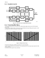
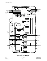
The 13 MHz system clock frequency is controlled by a 13-bit sigma-delta D/A in the OMEGA chip.

Figure 8.5:  AFC Block Diagram

8.6.

Audio

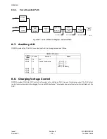
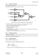
OMEGA provides the analogue interface for the digital audio samples processed by the DSP in HERCULES.

8.6.1.

Voice Uplink Path

Figure 8.6:  Voice ADC Block Diagram - Uplink Path


RINT1

RINT2

VTCXO

CEXT

AFC

3/5V

13-BIT DIGITAL

MODULATOR

1-BIT DAC

& LOW-PASS

FILTER

PROGRAMMATION REGISTER

OUTPUT SWING

CONTROL

10092-1

MICBIAS

MICIP
MICIN

AUXI

Bias

Generator

Microphone

Amplifier

Auxiliary

Amplifier

PGA

Sigma_Delta

Modulator

SINC

Filter

IIR

Bandpass

Filter

To voice

serial

interface

fs2=40KHz

fs3=8.0KHz

fs1=1MHz

10093-1

Summary of Contents for EB-GD93

Page 1: ...g Display Graphical chip on glass liquid crystal Alphanumeric 16 x 4 characters 2 lines of icons Illumination 4 LEDs for the LCD 7 colour 8 LEDs for the keypad Green 1 LED Incoming call Green 1 Charg...

Page 2: ...ation Industrial UK Ltd accepts no responsibility for inaccuracies which may occur and reserves the right to make changes to specification or design without prior notice The information contained in t...

Page 3: ...6 2 Keypad 19 6 3 Subscriber Identity Module 20 6 4 Time Processing Unit TPU 20 6 5 CPU Memory 21 6 6 LCD 21 6 7 Real Time Clock 21 6 8 Microphone 22 6 9 Speaker 23 6 10 Timers 24 6 11 UART 24 6 12 A...

Page 4: ...Issue 1 Section MCUK001001G8 Revision 0 iv Technical Guide This page is left intentionally blank...

Page 5: ...D93 personal cellular telephone operating on the GSM Digital Cellular Network 1 2 Structure of the Guide The manual is structured to provide service engineering personnel with the following technical...

Page 6: ...INTRODUCTION Issue 1 Section 1 MCUK001001G8 Revision 0 2 Technical Guide This page is intentionally blank...

Page 7: ...ET MPU nRESET signal 19 CS LCD LCD chip select signal HERCULES pin 14 20 GND Ground GND 21 BL 4 KEY Backlight ACC IC 49 22 VBAT Battery Voltage 23 KBR 4 Key Row 4 signal for Key scan HERCULES pin 179...

Page 8: ...ute 7 SERIAL UP Upward serial 9600 bps SMS cable 33 8 kbps Data adaptor I F Card up to 38 4 kbps Soft Modem cable 57 6 kbps Test Command 8 SERIAL DOWN Downward serial Baud rate same as SERIAL UP 9 ACC...

Page 9: ...MPWR TP623 HERCULES TX_IRDA TP624 HERCULES RX_IRDA TP625 HERCULES CLK32_OUT TP626 A28V TP627 D28VB TP628 D28V TP629 D18V TP630 D20V TP631 EARP TP632 EARN TP633 BAT_TEMP TP634 BAT_ID TP635 HF_TXAUDIO T...

Page 10: ...8 Revision 0 6 Technical Guide 2 2 2 Keypad PCB TP No Signal TP801 VBAT TP802 DS801 R801 TP803 DS802 R801 TP804 DS803 R802 TP805 DS804 R802 TP806 DS805 R803 TP807 DS806 R803 TP808 DS807 R804 TP809 DS8...

Page 11: ...ovide RF shielding A metallised plastic chassis has also been designed to provide smaller walled sections to isolate sensitive RF areas like the synthesiser block from high level interference such as...

Page 12: ...hi 2 GSM 270 MHz DCS 135 MHz GSM 270 MHz DCS 134 135 MHz GSM 1 160 1 185 MHz DCS Rx 1 580 1 655 MHz Tx 1 575 1 650 MHz RF Synthe RF VCO 1 160 1 185 MHz 1 575 1 655 MHz DCS 270 MHz GSM 540 MHz 270 MHz...

Page 13: ...tenna The antenna is a fixed helical type A mechanical switch is used to route the RF signal from the external antenna for handsfree operation and test purposes 3 2 4 Transmit and Receive The transmit...

Page 14: ...RF OVERVIEW Issue 1 Section 3 MCUK001001G8 Revision 0 10 Technical Guide This page is intentionally blank...

Page 15: ...CIES 1 5 6 10 11 15 16 20 21 25 890 200 891 200 892 200 893 200 894 200 890 400 891 400 892 400 893 400 894 400 890 600 891 600 892 600 893 600 894 600 890 800 891 800 892 800 893 800 894 800 891 000...

Page 16: ...is fed into the phase detector for the PLL modulation loop The output from the Tx VCO is fed in to the down conversion mixer It is mixed with the 1st LO output from the RF VCO and converted to the IF...

Page 17: ...itter Signal Levels 4 3 3 GSM 1800 Signal Levels The transmitter signal levels for the GSM 1800 band are as follows Figure 4 3 GSM 1800 Transmitter Signal Levels 50 0 30 0 10 0 10 0 30 0 VCO Splitter...

Page 18: ...TRANSMITTER Issue 1 Section 4 MCUK001001G8 Revision 0 14 Technical Guide This page is intentionally blank...

Page 19: ...38 400 939 400 935 600 936 600 937 600 938 600 939 600 935 800 936 800 937 800 938 800 939 800 936 000 937 000 938 000 939 000 940 000 26 30 31 35 36 40 41 45 46 50 940 200 941 200 942 200 943 200 944...

Page 20: ...h 900 MHz and 1800 MHz bands Note that the apprpriate signal path will be set by the Antenna switching module The output is applied to the internal dual LNA of the Bright III IC The Bright III LNA gai...

Page 21: ...from the mixers The DC level at the output of the operational amplifiers is 1 35 V with a 200 mV p p single ended AC swing controlled by the AGC loop to maintain optimum receiver signal levels 5 3 3 G...

Page 22: ...RECEIVER Issue 1 Section 5 MCUK001001G8 Revision 0 18 Technical Guide This page is intentionally blank...

Page 23: ...llocated an entire row of the keyboard scan The Keyboard scanning is software controlled Key pressed is indicated by an interrupt but key release is controlled by software SPI CPU CORE ROM RAM API PLL...

Page 24: ...FE 0004 REG_SIM_CONF1 SIM configuration register 1 Read Write FFFE 0006 REG_SIM_CONF2 SIM time delay parameters Read Write FFFE 0008 REG_SIM_IT SIM Interrupt status Read only FFFE 000A REG_SIM_DRX SIM...

Page 25: ...rcules uwire I F and one I O line assigned to distinguish command or data When sending data or commands the nSCS0 line is used for chip select To send data LCD_RS I O 3 is set high and to send command...

Page 26: ...ires that when in handheld mode the transmitter audio frequency response must fit within the mask shown below Figure 6 3 Handheld GSM Transmit Audio Frequency Response Mask When using a Handsfree acce...

Page 27: ...onse The telephonehas been designed to meet requirements with a Type 1 artificial ear 6 9 2 Desktop Handsfree DTHF A second speaker is mounted in the rear case for DTHF operation The GSM Standard requ...

Page 28: ...15 s and 20 649 s Timer 1 Function Buzzer Timer Setting Tone frequency Timer 2 Function N A Setting N A The timer unit registers are FFFF F800 Watchdog_CNTL_TIM Watchdog control 6 bit Read Write FFFF...

Page 29: ...ns four registers accessed via the serial interface R0 R1 and R2 are 8 bit write only registers R3 is an 8 bit read only register Serial Interface bit Bit function R0 Bit function R1 Bit function R2 B...

Page 30: ...able to read 1 ms after LOGIC_PWR bit is set to 1 This delay time is dependant on the ACC_PWR capacitance of the connected accessory D6 CHARGING_LED Not used PWM_ON nPHF_DETECT D5 BLCONT4 DTHF ON EN_U...

Page 31: ...t memory CPU clock speed is selectable and is set to achieve optimum speed for memory access For 90 ns access FLASH and RAM a 8 67 MHz clock gives no wait state access to both devices Debugging access...

Page 32: ...00 2k SIM interface 16 bits 0 TSP FFFE 0800 2k Timed Serial Port 16 bits 0 TPU REG FFFE 1000 1k GSM time registers 16 bits 0 TPU RAM FFFE 1400 1k GSM timing unit 16 bits 0 RTC FFFE 1800 2k Real Time C...

Page 33: ...tchdog Timer INT Edge sensitive IRQ1 Timer 1 INT Edge sensitive IRQ2 Timer 2 INT Edge sensitive IRQ3 OMEGA fast interrupt Low Level sensitive FIQ IRQ4 TPU frame INT Edge sensitive IRQ5 TPU page INT Ed...

Page 34: ...of timer 1 Ringing tones can be played by altering the value of timer 1 During melody ringer operation two output signals are controlled for clarity During Handsfree operation the ringing tone is der...

Page 35: ...DELTA SIGMA DELTA FILTER FILTER VOICEBAND SERIAL I F BASEBAND SERIAL I F MCU SERIAL I F MONITORING 10 BIT A D OMEGA SIM CARD INTERNAL REGISTERS SIGMA DELTA SIGMA DELTA BPF BPF LPF APC 10 Bit D A BATT...

Page 36: ...teristics The ramp time is selectable between each step being 1 16 of a bit and being 1 8 of a bit giving a maximum ramp time of either 14 77 s or 29 53 s An 8 bit value is used to program the ramp ou...

Page 37: ...igital audio samples processed by the DSP in HERCULES 8 6 1 Voice Uplink Path Figure 8 6 Voice ADC Block Diagram Uplink Path RINT1 RINT2 VTCXO CEXT AFC 3 5V 13 BIT DIGITAL MODULATOR 1 BIT DAC LOW PASS...

Page 38: ...ing control The DAC output is able to control accurately the charging for Li and NiMH batteries The telephone has electrical volume for calibration of this DAC OMEGA A D Inputs OMEGA Input Pin No Func...

Page 39: ...r amplifiers are powered directly from the battery VBAT 9 3 Power up 9 3 1 Power Modes The power up procedure has two phases If an initial check to see if the battery is in good condition is successfu...

Page 40: ...4 Power down There are two power down procedures The truth table for the power state transitions is shown below In some cases the phone does not power down completely but may enter a state of reduced...

Page 41: ...Power Source EB BSD93 battery packs use Lithium Ion cells which have the advantage of reduced weight size and improved gravimetric and volumetric densities compared to that of Ni MH cells Current mod...

Page 42: ...TO VOLTAGE CONVERTER MAIN BATTERY PRE CHARGE AND TRICKLE CHARGE BACKUP BATTERY CHARGE 1 4 scaling VCHG XTPWR ICHG Vcc3 VBAT VBACKUP BACKUP BATTERY Vcc1 FDBK VAUX Vcc2 VR2N UPR MAIN BATTERY DC DC CONVE...

Page 43: ...utput of the regulators and 13 MHz Clock to become stable Allow reset of HERCULES and OMEGA internal blocks 6 Set nRESET HIGH causing the ARM processor to start from address 0 9 5 4 Power Source Failu...

Page 44: ...are detected and the temperature is within specified limits the rapid charge algorithm is started Charging is determined by constant voltage and constant current control with time temperature and volt...

Page 45: ...DATA_ MODE0 4 DATA_ MODE 10 nACC_SENSE 5 EXT_PWR 13 ACC_PWR 9 High High High Low Low none High High High High Low AC DC Low Low Low Low High SMS cable Low High Low Low High DA High Low Low Low High S...

Page 46: ...Printed in UK UK001001500PJ...

Reviews: