background image


61


LTDVE4CH-20 | INSTRUCTIONS MANUAL 


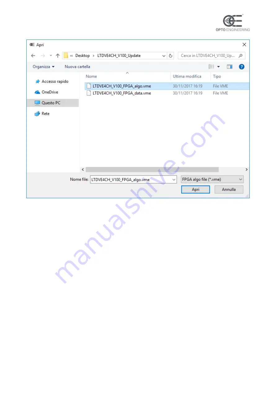
Figure 20: dialog used to locate the FPGA Algo firmware file 


After  the  FPGA Algo file has  been  specified, the  relative modal  dialog  is  closed. The  new  modal 
dialog of 

Figure 21: dialog used to locate the FPGA Data firmware file

 will then be displayed, asking 

to specify the FPGA Data file. 


Summary of Contents for LTDVE4CH-20

Page 1: ...ACCESSORIES INSTRUCTIONS MANUAL Strobe controller 4 CH LTDVE4CH 20...

Page 2: ...3 1 Light outputs 1 and 2 9 8 3 2 Light outputs 3 and 4 9 8 4 Input output synchronization 10 8 4 1 Synchronization inputs 10 8 4 2 Synchronization outputs 11 8 4 3 Serial RS485 interface 12 8 4 4 Ex...

Page 3: ...ters FILTER_SEL 0 3 35 14 2 8 Registers INPUT_SEL 0 7 35 14 2 9 Registers GEN_DLY_BASE 0 7 36 14 2 10 Registers GEN_DLY_CNT 0 7 37 14 2 11 Registers GEN_WDT_BASE 0 7 37 14 2 12 Registers GEN_WDT_CNT 0...

Page 4: ...5 14 2 43 Register SUPPLY_VOLTAGE 45 14 2 44 Registers MEASURED_CURRENT 0 3 45 14 2 45 Registers MEASURED_VOLTAGE 0 3 46 14 2 46 Register ERROR_WORD 46 14 2 47 Registers CALIB_CUR_ADD 0 3 47 14 2 48 R...

Page 5: ...etween any combination of applied signals must not exceed at all times the supply voltage Higher voltages may cause a fault and can be dangerous to human health This device has limited protection agai...

Page 6: ...necessary A digital input is used as a trigger When a rising edge on the trigger signal is detected the output is pulsed for the programmed amount of time Using this technique it is possible to obtain...

Page 7: ...atsink TempAmbient is the actual temperature of the ambient where the controller is placed ThResistence is the thermal resistance between the heatsink and the ambient For the LTDVE series the ThResist...

Page 8: ...l then changing the arrangement to series will increase the voltage across them but also reduce the overall current The last option feasible with this four channels controller would be to use two or m...

Page 9: ...n if equivalent mating plugs may be available these are the recommended components Connector designator Manufacturer Mating plug part number P1 P2 Phoenix Contact 1757035 P3 Phoenix Contact 1757022 P4...

Page 10: ...med P1and P2 It is possible to use two 2 way connectors in a 4 way socket The light output connections must not be paralleled or grounded in any way The state of each output is shown by a yellow LED i...

Page 11: ...outputs can be connected directly to the system for voltages up to 60V The state of each synchronization output is shown by a yellow LED indicator next to the connector Connector P4 also provides thre...

Page 12: ...ronization circuits Please note the reported values are typical Parameter Value Unit Note Uin low 0 1 V Uin high 3 3 24 V Iin 5 9 mA Internal constant current generator Table 6 specifications of input...

Page 13: ...es up to 60V Figure 3 interface circuits for output synchronization Circuit specifications are summarized in Table 8 specifications of output synchronization circuits Please note the reported values a...

Page 14: ...rnal temperature sensor in connector P4 These two analogue signals are not electrically isolated from the controller electronics Be careful not to connect them to any other signal A malfunction or sho...

Page 15: ...ontroller implements a subset of the Modbus RTU slave protocol and operates by default at 9600 bits per second with even parity The factory set Modbus address is 32 and it is saved in the controller n...

Page 16: ...nd LINK LEDs are identified by their position relative to the Ethernet RJ45 jack The ACT LED is at the left of the jack while the LINK LED is at the right Number Name Colour Description 1 PWR Green St...

Page 17: ...alues and the controller resumes normal operation During the ten seconds interval the RUN and ERR LEDs blink at a high rate to emphasize the circumstance In the meantime the use of the serial RS485 in...

Page 18: ...e relevant synchronization input with a finite state machine A change in the filter output is performed only when the input signal has remained constant for a defined period of time called filter time...

Page 19: ...synchronization input 4 TR4 Free running oscillator The free running oscillator is an autonomous asynchronous trigger source described in detail in the chapter 12 7 Setting of the input multiplexers...

Page 20: ...ht pulse generators can be entirely bypassed by selecting one of the four filtered synchronization inputs TR1 TR2 TR3 or TR4 Moreover the outputs can operate continuously by selecting the last option...

Page 21: ...appens when turn off time is too short As visible in the diagram the light is switched on at ToffMIN later than the original requirement Figure 9 protection prevents too short turn off time The four p...

Page 22: ...responding to a frequency of 1 Hz up to 100 Hz It can be selected as an input to the input multiplexers Common usage of the oscillator is to test the lights during machine assembly and deployment 13 W...

Page 23: ...the connections to the cameras because these are often vendor specific Please see the camera hardware manual for more information 13 2 Wiring example 2 camera triggers controller In the schematic dia...

Page 24: ...dbus became a well known communication protocol and it is now a commonly available means of connecting industrial electronic devices The development and update of Modbus protocols has been managed by...

Page 25: ...address of the register to be written and the actual data to be written Registers are addressed starting at zero The register data in the request message are packed as two bytes per register For each...

Page 26: ...14 INPUT_SEL0 RW 0 511 Setting of input multiplexer 1 15 INPUT_SEL1 RW 0 511 Setting of input multiplexer 2 16 INPUT_SEL2 RW 0 511 Setting of input multiplexer 3 17 INPUT_SEL3 RW 0 511 Setting of inpu...

Page 27: ...tor for generator 3 41 GEN_WDT_CNT2 RW 1 1023 Pulse width setting for generator 3 42 GEN_DLY_BASE3 RW 0 3 Pulse delay time base selector for generator 4 43 GEN_DLY_CNT3 RW 0 1023 Pulse delay setting f...

Page 28: ...elay time base selector for generator 8 59 GEN_DLY_CNT7 RW 0 1023 Pulse delay setting for generator 8 60 GEN_WDT_BASE7 RW 0 3 Pulse width time base selector for generator 8 61 GEN_WDT_CNT7 RW 1 1023 P...

Page 29: ...or LD2 output multiplexer 97 OUTPUT_SEL_LO1 RW 0 65535 Low order byte of setting for LD2 output multiplexer 98 OUTPUT_SEL_HI2 RW 0 511 High order byte of setting for LD3 output multiplexer 99 OUTPUT_S...

Page 30: ...UNUSED N A N A 125 UNUSED N A N A 126 PRT_CNT_ON0 RW 1 255 Maximum turn on time for LD1 127 PRT_ENA_ON0 RW 0 1 Enable limitation of turn on time for LD1 128 PRT_CNT_OFF0 RW 1 255 Minimum turn off time...

Page 31: ...UNUSED N A N A 156 UNUSED N A N A 157 UNUSED N A N A 158 CUR_RANGE0 RW 0 3 Current range for LD1 159 CUR_VALUE0 RW 0 20000 Current value for LD1 160 CUR_RANGE1 RW 0 3 Current range for LD2 161 CUR_VAL...

Page 32: ...65535 Bytes 6 and 7 of Ethernet host name 184 ETH_HOSTNAME4 RW 0 65535 Bytes 8 and 9 of Ethernet host name 185 ETH_HOSTNAME5 RW 0 65535 Bytes 10 and 11 of Ethernet host name 186 ETH_HOSTNAME6 RW 0 655...

Page 33: ...ord 204 WEB_PASSWORD2 RW 0 65535 Bytes 4 and 5 of web password 205 WEB_PASSWORD3 RW 0 65535 Bytes 6 and 7 of web password 206 BOARD_TEMPERATURE0 R 200 to 1000 Board temperature next to LD1 and LD2 dri...

Page 34: ...D1 current measurement 231 CALIB_CUR_ADD1 R 0 65535 Calibration constant for LD2 current measurement 232 CALIB_CUR_MUL1 R 0 65535 Calibration constant for LD2 current measurement 233 CALIB_CUR_ADD2 R...

Page 35: ...use 511 BOARD_COMMAND RW 0 3 Board command Table 15 controller register file As indicated in the table most of the registers can be both read and written type RW some registers are read only type R an...

Page 36: ...ld 15 10 of this register is unused When writing these bits they must be set to zero 14 2 7 Registers FILTER_SEL 0 3 Each bit field 2 0 of these four registers selects the time constant for filtering...

Page 37: ...gisters holds the time base selector for the generation of the pulse delay in the relevant pulse generator GEN_DLY_BASE0 time base selector for generation of pulse delay in generator 1 GEN_DLY_BASE1 t...

Page 38: ...s are unused When writing these bits they must be set to zero 14 2 11 Registers GEN_WDT_BASE 0 7 Each bit field 1 0 of these eight registers holds the time base selector for the generation of the puls...

Page 39: ...ltiplexers are used to route the internal signals to the light outputs and synchronization outputs Each output multiplexer has an independent selector The selector of a specific output multiplexer is...

Page 40: ...t fields 8 0 the nine high order bits of the selectors while registers OUTPUT_SEL_LO x hold the remaining sixteen low order bits of the selectors OUT_SEL_LO0 lower sixteen bits of output multiplexer 1...

Page 41: ...urn off time for light output LD1 PRT_CNT_OFF1 minimum turn off time for light output LD2 PRT_CNT_OFF2 minimum turn off time for light output LD3 PRT_CNT_OFF3 minimum turn off time for light output LD...

Page 42: ...m zero up to 20000 mA The resolution of the generated current depends on the range the required current falls in Please see section 4 2 for more information Avoid operation with non allowed values Bit...

Page 43: ...ee chapter 11 for a description of the INIT button functionalities Note the current firmware supports only even parity 14 2 24 Registers ETH_MAC_ADDR 0 2 These registers contain the Ethernet MAC addre...

Page 44: ...55 0 The factory settings can be restored using the INIT button see chapter 11 for a description of the INIT button functionalities 14 2 30 Register ETH_SUBNET_MASK_LO This register contains the sixte...

Page 45: ...of the INIT button functionalities 14 2 37 Register ETH_MODBUS_ADDR This register contains the Modbus address of the controller for the Ethernet interface The default value is 32 Permitted values are...

Page 46: ...as signed sixteen bits integers with a resolution of 0 1 C Given a register value the corresponding actual temperature for a couple of power stages can be calculated as follows BoardTemperature x C va...

Page 47: ...ges reset if safe temperature Bit 2 set if excessive temperature on LD3 and LD4 output stages reset if safe temperature Bit 5 set if LD1 output stage has been disabled reset if LD1 output stage is act...

Page 48: ...ut LD1 voltage CALIB_CUR_ADD1 calibration constant for measurement of light output LD2 voltage CALIB_CUR_ADD2 calibration constant for measurement of light output LD3 voltage CALIB_CUR_ADD3 calibratio...

Page 49: ...cription of the INIT button functionalities For more information about the Modbus RTU Modbus TCP and Modbus UDP protocols and the Modbus register file please refer to chapter 14 1 and chapter 14 2 To...

Page 50: ...on menu that is used to access all the other pages necessary to configure and manage the controller The navigation menu is always visible and accessible at the top of every page From the navigation me...

Page 51: ...d current LD1 measured current on light output LD1 o Measured current LD2 measured current on light output LD2 o Measured current LD3 measured current on light output LD3 o Measured current LD4 measur...

Page 52: ...filter is enabled with a 10 s time constant 20 s the filter is enabled with a 20 s time constant 50 s the filter is enabled with a 50 s time constant 100 s the filter is enabled with a 100 s time cons...

Page 53: ...chosen between Off default Input TR1 Input TR2 Input TR3 Input TR4 and Oscillator When set to Off the generator is disabled When set to Oscillator the internal free running oscillator is used as the...

Page 54: ...to the pulse generators from 5 to 8 Please refer to the description of page Setup pulse generators GN1 GN4 in chapter 14 3 3 for more information 14 3 5 Setup light outputs LD1 LD4 This page allows t...

Page 55: ...nst excessive turn on time and protection against insufficient turn off time can be independently enabled or disabled for each light output Source selects the activation source for the light output It...

Page 56: ...t excessive turn on time Ton max is the maximum turn on time for the connected light expressed in ms The maximum turn on time may range from 1 ms to 255 ms with a resolution of 1 ms Toff check enables...

Page 57: ...erator GN8 Input TR1 Input TR2 Input TR3 Input TR4 and Continuous When set to Off the synchronization output is disabled When set to Continuous the synchronization output is always active 14 3 7 Gener...

Page 58: ...matches the saved password the settings can be changed In case the entered password does not match the saved password the settings are displayed but they cannot be changed The password can be modifie...

Page 59: ...the TCP port used for the Modbus TCP protocol Modbus UDP port is the UDP port used for the Modbus UDP protocol The fields under RS485 interface collect all the settings related to the serial RS485 in...

Page 60: ...he new password to be used repeated for safety Maximum length for the password is eight characters The password is cleared when the settings are reset to the factory settings using the INIT button see...

Page 61: ...re updater application presents the main window of the PC application Figure 19 main window of LTDVE firmware updater application It is necessary to specify the communication port on the PC the contro...

Page 62: ...locate the FPGA Algo firmware file After the FPGA Algo file has been specified the relative modal dialog is closed The new modal dialog of Figure 21 dialog used to locate the FPGA Data firmware file...

Page 63: ...pecified the relative modal dialog is closed The couple of FPGA firmware files will then be loaded from the PC disk to the PC RAM The text box at the bottom of the main window will then be updated wit...

Page 64: ...are files have been loaded To update the MCU firmware it is necessary to specify a single file named the MCU file After pressing the Load MCU file button the modal dialog of Figure 23 dialog used to l...

Page 65: ...will then be loaded from the PC disk to the PC RAM The text box at the bottom of the main window will then be updated with some information regarding the loading process see image in Figure 24 main wi...

Page 66: ...e progress bar in the middle of the main window keeps updating to show the advancement of the process The text box at the bottom of the main window is updated with more information regarding the updat...

Page 67: ...GA Algo firmware is transferred see image in Figure 27 FPGA Algo firmware update sequence Figure 27 FPGA Algo firmware update sequence The FPGA is programmed just after both the FPGA Data and the FPGA...

Page 68: ...A programming The information in Figure 29 main window after successful firmware update is displayed when the update process is successfully finished Figure 29 main window after successful firmware up...

Page 69: ...68 LTDVE4CH 20 INSTRUCTIONS MANUAL...

Reviews: