EVBUM2822/D
2
TYPICAL APPLICATION SCHEMATIC
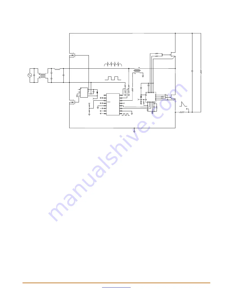
Figure 2. Typical Application Schematic of a CrM Totem Pole PFC Utilizing NCP1680
VL
VAC
+
_
NCP51530
HI
LI
COM
LO
VCC
HB
HO
VB
ZCD
SR2
SR1
NCP1680
POLARITY
PWMH
LVSNS1
PFCOK
FB
LVSNS2
PWML
SRH
ZCD
PGND
SKIP
FAULT
VCC
R
AUX
0 V
+400 V
+
+
+
−
−
+
+
+
−
−
Vac
400
−
Vac
V
O
V
O
R
LOAD
R
ZCD
AUX
VCC
SRL
SRH
SRL
NCP51820
VDD
VBST
SW
HOSRC
VDDH
HOSNK
LOSRC
VDDL
PGND
LOSNK
HIN
LIN
SG
ND
EN
DT
S1
S2
VCC
GND
VCC
As shown in Figure 2, the slow leg switches (SR1 & SR2)
are high voltage silicon
−
based FETs, also known as super
junction (SJ) FETs, and the fast leg switches (S1 & S2) are
Enhancement
−
mode Gallium Nitride (eGaN) devices. Since
NCP1680 employs a CrM control architecture where the
inductor current resets back to zero before the next
switching cycle, low reverse recovery charge (Qrr) SJ FETs
can also be utilized for the fast leg albeit with slightly
inferior performance, but better cost structure. As
a controller the NCP1680 is agnostic to the fast leg switch
technology. Wide
−
Bandgap (WBG) devices such as Silicon
Carbide (SiC) or eGaN are recommended for optimal
performance. SiC is a good choice for lower frequency
applications while eGaN is an excellent choice for both low
frequency and high frequency applications.
The NCP1680 evaluation board is designed such that
engineers interested in this novel topology can easily probe
various signals and learn the intricacies of TPFC. The fast
leg half bridge is implemented on a daughter card where the
fast leg switches are driven using NCP51820, a high voltage
eGaN half
−
bridge driver; the slow leg switches are driven
using NCP51530, a high voltage Si FET half
−
bridge driver.
The NCP1680 employs a novel current limit scheme where
a simple resistor placed in the return path between bulk
ground and the IC ground, is utilized for current limiting.
The Zero Current Detection (ZCD) resistor is further
utilized for drive control of the synchronous switch in the
fast leg.
Additionally, the NCP1680 requires only a single
auxiliary winding to sense switch node valleys (in positive
half
−
line cycle) and switch node peaks (in negative half line
cycle). This novel scheme results in the main boost switch
being turned on with minimal voltage across the switch
improving efficiency and reducing EMI.
Summary of Contents for NCP1680
Page 12: ...EVBUM2822 D www onsemi com 12 MOTHERBOARD PCB ARTWORK Figure 17 Motherboard PCB Part 1 3...
Page 15: ...EVBUM2822 D www onsemi com 15 DAUGHTERBOARD PCB ARTWORK Figure 20 Daughterboard PCB Part 1 2...
Page 17: ...EVBUM2822 D www onsemi com 17 TRANSFORMER DATA SHEET Figure 22 Transformer Data Sheet...
Page 19: ...EVBUM2822 D www onsemi com 19 Daughter Card Figure 25 Daughter Card...


