Global Support&Service Department
OLYMPUS IMAGING CORP.
Ver.1
- INDEX -
REPAIR MANUAL
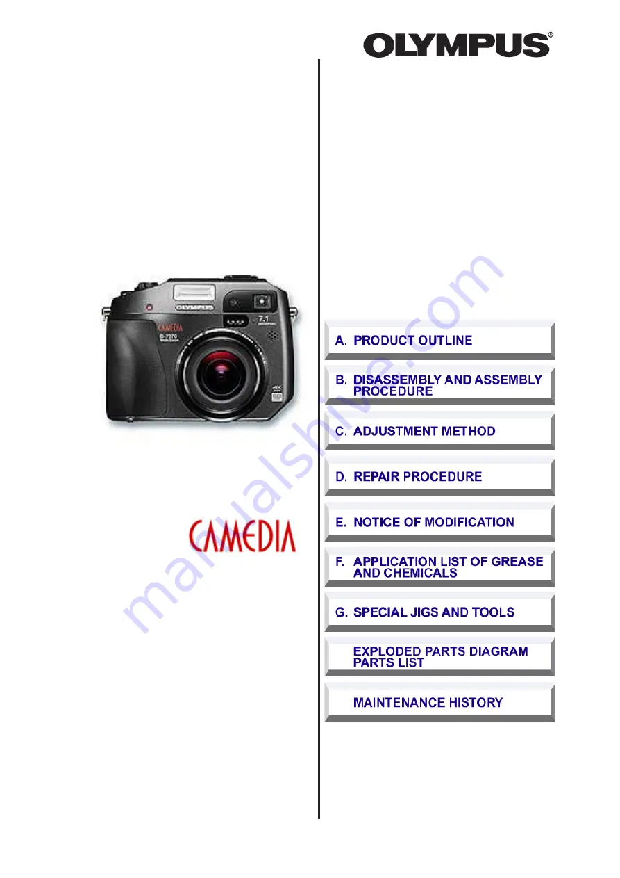
C-7070 Wide Zoom
Page 1: ...Global Support Service Department OLYMPUS IMAGING CORP Ver 1 INDEX REPAIR MANUAL C 7070 Wide Zoom...
Page 2: ...Resolutions and Number of storable photos A 3 Image Adjustment Modes Function Shooting Sequence ViewFinder LCD Focusing System Focusing ranges A 4 Exposure Control Metering System White Balance Syste...
Page 3: ...ult F G S PAL C 7070 Wide Zoom G General E default K SC TC PAL C 7070 Wide Zoom K Korea E default K SC TC PAL C 7070 Wide Zoom H HongKong E default K SC TC PAL C 7070 Wide Zoom A Oceania E default K S...
Page 4: ...2 frames SQ1 8 frames SQ1 25 frames 2288 x 1712 TIFF 2 frames SQ1 11 frames SQ1 32 frames 2048 x 1536 TIFF 3 frames SQ1 13 frames SQ1 40 frames 1600 x 1200 TIFF 5 frames SQ2 22 frames SQ2 64 frames 1...
Page 5: ...ge Adjust ment Modes Sequence 1 4 fps HQ max 10 images Hi speed 2 5 fps max 2 images ViewFinder Electronic viewfinder LCD 1 8 inch Semi Transmissive swivel LCD 130 000 pixel Focusing System Autofocus...
Page 6: ...icture Card 16 32 64 128 256 512MB Compact Flash Type I or Type II 4MB 8GB Microdrive 1GB Remote Control Yes White Balance System Auto iESP2 Pre set shade overcast sunlight evening sun fluorescent lig...
Page 7: ...rees 90 degrees Slideshows Motion image Nomal Reverse Frame by frame Fast Forward Rewind Size W 116 mm x H 87 mm x D 65 5 mm Weight 433 g without battery and media card Auto connect USB Compatible wit...
Page 8: ...CEDURE 1 REMOVAL OF CABINET BACK AND CABINET FRONT B 2 2 REMOVAL OF CABI TOP AND CP1 BOARD B 3 3 REMOVAL OF PW2 BOARD LENS ASSEMBLY CA1 BOARD PW1 BOARD AND ST1 BOARD B 4 4 REMOVAL OF TB3 BOARD LCD VF1...
Page 9: ...1 7 x 3 5 7 Screw 2 x 3 8 Screw 1 7 x 4 9 Open the cover USB 10 Open the cover DC jack 11 Two screws 1 7 x 3 5 12 Open the cover card 13 Two screws 1 7 x 4 14 Open cabinet back a little Be careful abo...
Page 10: ...4 Discharge 5 Two screws 1 7 x 4 6 Connector 7 Compl cover jack 8 Connector 9 Microphone 10 Remove the solder 11 Six FPCs 12 Two screws 1 7 x 3 5 13 Cover terminal 14 Remove FPC from boss 15 Two screw...
Page 11: ...gear 15 Gear FK idle 16 Washer 17 FK gear 18 Three screws 1 7 x 4 19 Two screws 1 7 x 3 20 Lens assembly 21 Three screws 1 7 x 5 22 Lens VF 23 PW1 board 24 Flexible CA1 to CP1 25 Three screws 1 7 x 4...
Page 12: ...3 board 5 Four screws 1 7 x 3 6 Cover back LCD 7 FPC 8 Connector 9 Two screws 2 x 3 5 10 Cover front LCD 11 LCD 12 Holder LCD 13 Remove the solder 14 VF1 board 15 Spacer LCD 16 Screw 1 7 x 2 17 TB1 bo...
Page 13: ...B 6 Ver 1 B DISASSEMBLY AND ASSEMBLY PROCEDURE C 7070WideZoom 5 BOARDLOCATION TB2 board TB3 board TB1 board VF1 board CP1 board ST1 board PW1 board PW2 board CA1 board...
Page 14: ...6 USB STORAGE INFORMATION REGISTRATION C 4 7 ADJUST SPECIFICATIONS C 5 1 AF LED ANGLE ADJUSTMENT C 5 2 LENS ADJUSTMENT C 6 3 AWB ADJUSTMENT C 7 4 CCD WHITE POINT DEFECT DETECT ADJUSTMENT C 7 5 CCD BLA...
Page 15: ...ts Windows 98SE or ME or 2000 or XP IBM compatible PC with pentium processor CD ROM drive 3 5 inch high density diskette drive USB port 40 MB RAM Hard disk drive with at least 15 MB available VGA or S...
Page 16: ...C 7070 Wide Zoom 5 Connecting the camera to the computer 1 Line up the arrow on the cable connector with the notch on the camera s USB port Insert the connector 2 Locate a USB port on your computer AC...
Page 17: ...he Get button in the USB storage window and check the USB storage data VID OLYMPUS PID C7070WZ Serial Rev 1 00 4 Check the Serial in the above USB storage data If the displayed value is different from...
Page 18: ...Carry out the pre focus adjustment After adjusting the target mark will appear on the monitor 6 Turn off the light of target board 7 Turn the screws on FPC unit to adjust so that the cen ter of the L...
Page 19: ...h ON Setting of pattern box Color temperature 3100 20 K Luminance 900 20 cd m2 Adjusting method 1 Set the camera 0 cm from the pattern box Do not enter any light 2 Double click on the DscCalDi exe 3 C...
Page 20: ...oint Defect Detect Adjustment In Lighted 6 PAF Adjustment 6 1 Uniform Adjustment Preparation POWER switch ON Setting of pattern box Color temperature 3100 20 K Luminance 900 20 cd m2 Note Orient the P...
Page 21: ...ons Adjustment value determination Ideal value of LEFT optic axis difference L3 8 Acceptable value of LEFT optic axis difference L3 ideal value 10 18 2 Ideal value of RIGHT optic axis difference R3 14...
Page 22: ...m and maximum values is 1 0 or more 4 The adjustment is OK if the camera is moved and then the difference between the minimum and maximum val ues is within 1 0 7 LCD Panel Adjustment VF1 board Side B...
Page 23: ...ied out first CL413 waveform VG CL414 waveform VG 0 05 0 1 Vp p CL411 waveform 3 6 V 0 1 Vp p 7 5 LCD Blue Brightness Adjustment Adjusting method 1 Adjust LCD B Bright so that the amplitude of the CL4...
Page 24: ...the power switch CARD COVER OPEN will be displayed in the LCD 3 Push the LCD button and OK button more than 3 sec onds simultaneously 4 Push the right arrow button and select CONTROL 5 STORAGE CONTROL...
Page 25: ...Offset Adjustment 7 3 LCD Gain Adjustment 7 4 LCD Red Brightness Adjustment 7 5 LCD Blue Brightness Adjustment 7 6 LCD VcomPP Adjustment Adjustment items Changed repair parts 9 Notice after adjustment...
Page 26: ...C 13 Ver 1 C ADJUSTMENT METHOD C 7070 Wide Zoom...
Page 27: ...Ver 1 D 1 C 7070 Wide Zoom D REPAIR PROCEDURE 1 TROUBLESHOOTING GUIDE D 2 2 CONFIRMATION AND UPDATE OF THE FIRMWARE D 3...
Page 28: ...IC301 6 BAT OFF CHECK R3019 IC301 20 4MHz OSCILLATION CHECK X3001 IC301 16 32 768kHz OSCILLATION CHECK X3002 R3006 C3010 C3012 CHECK IC301 PUSH SHUTTER BUTTON IC301 90 91 SCAN IN 0 1 PULSE INPUT CHECK...
Page 29: ...rd which was formated in C 7070 Wide Zoom and save the binary data firmware bin into the folder Firmware 2 Camera is operated by AC adapter Do not operate with battery Insert the F W card for C 7070 W...
Page 30: ...E 1 Ver 1 C 7070 Wide Zoom E NOTICE OF MODIFICATION...
Page 31: ...F 1 Ver 1 C 7070 Wide Zoom F APPLICATION LIST OF GREASE AND CHEMICALS...
Page 32: ...G 1 Ver 1 C 7070 Wide Zoom G SPECIAL JIGS AND TOOLS...
Page 33: ...7070 Wide Zoom H DESCRIPTION OF MECHANISM 1 CA1 CIRCUIT DESCRIPTION H 2 2 CP1 AND VF1 CIRCUIT DESCRIPTION H 5 3 PW1 POWER CIRCUIT DESCRIPTION H 6 4 ST1 STROBE CIRCUIT DESCRIPTION H 7 5 SYA CIRCUIT DES...
Page 34: ...iption SUB GND DC 0 V Aprox 10 V Aprox 8 V 12 5 V 16 V When sensor read out Fig 1 2 CCD Block Diagram 1 CA1 CIRCUIT DESCRIPTION 1 IC Configuration IC902 ICX489AQF CCD imager IC991 IC992 CXD3440EN V dr...
Page 35: ...G signal which is output from pin 21 of IC906 is the reset gate clock 4 IC906 CDS AGC Circuit and A D Converter The video signal which is output from the CCD is input to pins 27 of IC906 There are S H...
Page 36: ...The electric charges sent to the final stage of the horizontal CCD are transferred to the floating diffusion as shown in Fig 1 5 RG is turned on by the timing in 1 and the floating diffusion is charg...
Page 37: ...a is to be output to an external device it is taken data from the memory When played back on the LCD and monitor data is transferred from memery to the SDRAM and the image is then elongated so that it...
Page 38: ...f output is short circuited for the length of time determined by the condenser which is connected to Pin 37 of IC501 all output is turned off The control signal P ON are re controlled to restore outpu...
Page 39: ...t by the oscillation transformer 1 5 Rectifier circuit The high voltage alternating current which is generated at the secondary side of T5401 is rectified to produce a high voltage direct current and...
Page 40: ...put 1 4 LCD segment output 0 18 CARD lid switch detection AV JACK insertion detection Jog dial B detection signal Microprocessor card rewriting port ASIC serial communication requirement System reset...
Page 41: ...5 SI I Serial communication data input ASIC 96 AVSS GND 97 100 SCAN IN 6 3 I Key matrix input Expansion memory card CF attachment detection signal L Attachment 85 O DC DC converter ON OFF signal H ON...
Page 42: ...battery for backup is charged 10 hours from it to be attached When the power switch is on the 8 bit microprocessor starts processing The 8 bit microprocessor first sets both the PON signal at pin 85 a...
Page 43: ...N I 3 SYSYEM CONTROL I 4 CCD I 5 LENS I 6 POWER I 7 STROBO I 8 CUIT DIAGRAMS I 9 OVERALL I 9 CP1 DMA I 10 CA1 I 11 CP1 SYA I 12 CP1 TCA I 13 PW1 PW2 I 14 VF1 TB1 I 15 TB2 TB3 I 16 ST1 I 17 MOUNTING DI...
Page 44: ...iver LCD Driver E lectoronic Flash S T1 BLOCK PW1 BLOCK S IO Y 48 0MHz U V AV S PE AKE R JACK 2 3 4 1 V OUT MIC Y C CF Card VF1 BLOCK Back light LCD Display 1 8inch US B 3 2 PON Power S upply 8bit D A...
Page 45: ...T COMPACT FLAS H LE NS 4 CN951 CN952 IC142 IC143 CN901 CA1 BOAR D CCD BLOCK IC991 IC992 CXD3440E N CCD V DR IVE R R E G CN541 CN501 PAF UNIT TOP FPC UNIT R XD0 IR IN IR IN R XD2 AUDS D AUDC K AUDLD S...
Page 46: ...E 2 PAF THE R M PAFTH 68 JOG B JOG B 7 JOG A JOG A S R E Q S DO S DI S CK MR S T PON PAON TO DMA B AT OF F AL3 2V UNR E G VDD R E S E T A MOVIE S CE NE TE LE My WIDE S HUTTE R 2nd LCD OPE N ALWAYS 3 2...
Page 47: ...99 XS G2A 96 XS G2B 95 XS G2C 94 XS G3A 93 XS G3B 92 XVS 90 XVH 91 XS UB 71 Q9002 IC909 TK11330CS 3 0V 3 45V A V DD3 AD9949 27 CCD IN 21 15 19 14 18 19 27 H1B H1A IC991 V DR IVE R CXD3440E N 1 3 5 6...
Page 48: ...IC101 266pin PIS W2 P IC101 269pin IIN1 IC101 278pin IIN2 IC101 277pin IIN3 IC101 276pin IIN4 IC101 275pin WS W IC101 239pin FPI IC101 244pin ZPULS E IC101 245pin FIN1 IC101 274pin FIN2 IC101 273pin...
Page 49: ...CUIT L5111 Q5111 S TE P UP CIR CUIT VM VM_LIM 15 0V A 7 5V A 3 45V A 1 25 D 3 25V D 8 5V L AFLE D_V LCD ANODE LCE CATHODE VM_S W LCD ON P ON P A ON LCD BL 31 29 11 9 15 18 28 27 13 12 8 5 25 26 24 23...
Page 50: ...FILTE R BLOCK Q5405 D5407 Q5407 OS CILLATION CIR CUIT E MIS S ION CONTR OL CIR CUIT OS CILLAION TR ANS FOR ME R R E CTIFIE R CIR CUIT VOLTAGE MONITOR CIR CUIT Q5409 LIGHT E MIS S ION CIR CUIT CHAR GI...
Page 51: ...SCAN IN 6 SCAN IN 5 ALWAYS3 2V JOG B JOG A SCAN IN 6 SCAN IN 3 SCAN IN 1 SCAN IN 2 SCAN IN 4 SCAN IN 5 SCAN IN 0 SCAN OUT 4 SCAN OUT 5 SCAN OUT 1 SCAN OUT 3 CARD_LED SCAN OUT 0 S15 S26 S25 S24 S23 S2...
Page 52: ...D0 SD3 SD2 SD5 SD4 SD6 SD1 ZCS0 D10 D9 D8 ZFRD A1 D0 D1 D2 SD14 SD12 SD13 SD9 SD11 SD10 SD15 SD21 SD20 SD22 SD18 SD19 SD17 SD16 ASIC V ASIC U SD30 SD25 SD27 SD26 SD29 SD28 SD31 J TE S T1 MR S T COMREQ...
Page 53: ...C B901 C 9019 IC909 RB901 R9066 R9068 C 9067 C 9069 R9069 R9067 R9073 R9071 C9065 R9074 R9070 R9072 51 51 100 K 1 H 470 1 16J 0 1 16Z 10 B 82K 1 16J 10 B 2 2K 1 16J 2SC3931 ICX489AQF 3 9 1 16J 1 2K 1...
Page 54: ...S 18 S 20 S 21 S 22 S 23 S 24 S 25 S 26 S 27 S 28 S 29 PAON PON AL3 2V S3 S2 S8 S6 S7 S12 S10 S9 S11 S4 S5 S13 S14 SI0 SI1 SI2 SO5 LCDBL TO DMA LCDON ZPULSE RXD0 IRIN PAFTH SI5 SI4 SI6 SI0 SI1 SI2 SI...
Page 55: ...I PISW1 PISW2 P WSW SIN2 SIN1 FIN4 FIN3 FIN2 FIN1 SIN1 SIN2 VCTRL R B953 Q9509 C9520 CN951 C9530 R 9508 Q9501 R B952 CB951 C9518 IC956 C9514 C9519 R9518 C 9516 R9519 D9503 C9517 R 9520 C9515 CN952 R 9...
Page 56: ...VR501 R5095 C 5112 R 5193 C5018 C5016 C5017 C 5132 Q5131 L5131 R5134 R5136 R 5137 R5135 C 5133 D5131 Q5132 R 5133 R 5132 C B501 R 5155 R 5158 R 5157 R 5160 R 5159 R5156 C 5153 R5154 D5151 EMX1 10K 1...
Page 57: ...1703 R 1711 L1751 R 1734 CN172 C1733 L1701 C 1704 R1702 R 1704 R1735 C 1710 C 1748 C B171 C1718 R B171 C1713 R 1708 C 1743 IC173 C 1778 R1741 C1741 Q1705 C 1759 R 1732 R 1733 CN171 C 1702 R 1714 C 175...
Page 58: ...JOGB JOGA JOGB SI3 SI4 D6501 CN651 CN652 CN653 S6502 S6507 S6505 S6504 S6508 S6509 S6501 D6504 D6503 D6502 D6505 CN654 S6503 S6506 DMA4S111 11 2 SKQGAB SKQGAB SKQGAB SKQGAB SKQGAB SKQGAB SKQGAB DMA6S...
Page 59: ...C5411 CN541 T5401 Q5407 C5403 C 5407 D5402 C 5401 R 5409 C 5406 R 5413 D5407 Q5405 R5406 R5408 R5414 R5423 R 5426 D5408 Q5409 D5409 C 5416 C5414 R5430 R5401 C 5415 IC541 Q5401 R5421 R5432 Q5406 D5406...
Page 60: ...162 C1056 R 1051 R1053 R 1041 R 1052 R 1042 R 1036 R1037 R 1034 R 1035 R 1038 R 1030 R 1065 R 1066 R 1069 R 1070 R 1068 C1014 C1013 R1012 R 1043 R 1045 R 1062 R1064 C1077 R 1073 R 1072 R 1067 R 1060 C...
Page 61: ...5 D5172 C5044 C5043 Q5042 R5042 R5041 R 5044 C5047 C5201 R5043 C5009 CN502 F5002 D5044 D5041 D5042 T5001 D5043 C5171 L9601 L5071 L5091 L5111 L5131 D5072 R 9605 RB501 CN501 C5092 C5072 L5176 L5175 R 54...
Page 62: ...Global Support Service Department OLYMPUS IMAGING CORP Maintenance History MODEL C 7070 Wide Zoom 1 1 No Date of issued Page Detail Ver 1 2005 02 04 1 set Initial...
Page 63: ...0 VE089300 VE210000 VE209800 VC245100 VC245900 VC246700 VC245700 VC245600 VC245500 VC242700 VG127700 VC243800 VG127600 VG125400 VG125300 VC247500 VG125500 VC248600 VC248300 VC195000 VE147700 VC245400...
Page 64: ...00 VG126100 VG128400 VG128500 VC247100 VG126200 VC193000 VG126300 VC272800 VG129000 VG128600 VG084900 VG084900 VG084900 VG129100 VG084900 VG084800 VG084800 VG129300 VG129200 VG128800 VG125600 VG125700...
Page 65: ...G131100 VC242300 VG131200 VC242500 VC241400 VG131000 VC242800 VC243900 VG074400 VC243700 VG130100 VG130200 VG130300 VC241200 VC899100 VC241300 VC242600 VC241500 VC240400 VC241700 VG128900 VG128900 VG1...
Page 66: ...C MONITOR LCD 2 D1 VC243700 SPACER 3 D3 VC243800 SPACER SPEAKER 1 D3 VC243900 SPACER LPF 3 D3 VC244000 SPACER LENS R 3 C4 VC244100 HOLDER CHASSIS 3 B4 VC244200 SPACER LENS U 3 B4 VC244300 ADHESIVE FPC...
Page 67: ...H TB 2 S6509 VC861500 SWITCH PUSH TB 2 JK112 VC866000 JACK PHONE D3 6 AV JACK CP 1 Z3001 VC880300 BATTERY RECHARGE CP 1 S6701 VC881500 SWITCH PUSH 1P 1TX1 TB 3 S3001 VC892600 SWITCH DETECTOR 1P 1T CP...
Page 68: ...DHESIVE GRIP L 1 A2 NEW VG128100 ADHESIVE HOLDER GRIP 1 A2 NEW VG128200 EARTH FRONT 1 D1 NEW VG128300 SPACER FPC CABI B 2 C3 NEW VG128400 SPACER TB2 2 A4 NEW VG128500 SHIELD TAPE TB2 2 A4 NEW VG128600...
Page 69: ...PAN PCS 1 7X3 3 A1 etc NEW VG131600 SPECIAL SCREW 1 7X9 3 B2 NEW VG131700 SCR S TPG PAN PCS 1 7X3 5 3 B3 NEW CN110 VG131800 SOCKET USB CP 1 NEW F5004 VG131900 FUSE 32V 1 5A PW 1 NEW JK501 VG132000 SO...