


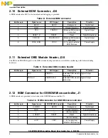


2.10 External BDM Connector, J34
A BDM interface for MCU code download and debugging is provided.
Table 8. External BDM connector
Interface pin
Signal name
MCU signal
Description
Direction
1
BKGD
BKGD
Background
Digital Input
2
GND
—
Ground reference
Power Reference
3
PDO
PS5/PDO
Extended DBG module
data output
Digital Output
4
RESET_B
RESET
Reset
Digital Bidirectional
5
PDOCLK
PS4/PDOCLK
Extended DBG module
data clock
Digital Output
6
VDDX_BDM
VDDX
5 V supply to external
BDM interface
Power Supply
2.11 Extended DBG Module Header, J38
The PDO and PDOCLK signals to the DBG extended debug module are available for interfacing with dedicated debug
hardware.
Table 9. Extended DBG module header
Interface pin
Signal name
MCU signal
Description
Direction
1
PDO
PS5/PDO
Extended DBG module
data output
Digital Output
2
PDOCLK
PS4/PDOCLK
Extended DBG module
data clock
Digital Output
2.12 BDM Connector for OSBDM Microcontroller, J1
A BDM interface is provided to load code to the OSBDM microcontroller, U1.
Table 10. BDM connector for OSBDM microcontroller
Interface pin
Signal name
OSBDM MCU signal
Description
Direction
1
U_BKGD
BKGD
Background
Digital Input
2
GND
—
Ground reference
Power Reference
3
—
—
(Not connected)
—
4
U_RESET
RESET
Reset
Digital Bidirectional
5
—
—
(Not connected)
—
6
+5 VU
VDD1
5 V supply from
OSBDM USB interface
Power Supply
Interface Description
S12ZVM12EVB Evaluation Board User Guide, Rev. 2, 03/2016
8
Freescale Semiconductor, Inc.