
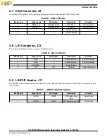


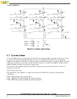
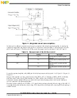


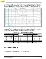


Figure 12. Phase A/DC Bus current sense option
With the sense resistor value of 10 milliohms, and the gain being 12.5, the maximum excursion of +/- 2.5 V from the mid-
range voltage of 2.5 V corresponds to a sensed current of 20 A:
Vamp, max = +/-2.5 V
Vsensed, max = (Vamp, max) / Gain = (+/-2.5V) / 12.5 = 0.2 V
Isensed, max =( Vsensed, max) / Rsense = (+/-0.2V) / 0.01ohm = +/- 20 A.
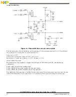
Option 2) Internal Op-Amp 1:
The internal current sense amplifier 1 is mapped to the ADC pins at PAD5, PAD6, and PAD7, with the following
configuration:
PAD5 = AMP1, the operational amplifier output.
PAD6 = AMPM1, the operational amplifier inverting input (minus).
PAD7 = AMPP1, the operational amplifier non-inverting input (plus).
This amplifier has fixed connections to the Phase B current sense resistor. The external gain setting resistors have the same
values as described before. It is also connected to a 2.5 V reference to allow for positive and negative current swings.
Design Considerations
S12ZVM12EVB Evaluation Board User Guide, Rev. 2, 03/2016
20
Freescale Semiconductor, Inc.