


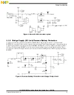


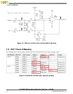


3.2.3 Charge Pump for High-Side Driver Supply
before, the first charge pump drives the N-channel MOSFET for reverse battery protection based on components D25, D26,
C34 and C107. The second charge pump, composed of C35, C40, D16, and D17, feeds a voltage into the MCU, through the
VCP pin.
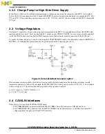
3.3 Voltage Regulators
The main 5 V regulator is a linear voltage regulator integrated into the MCU. It is supplied directly from the VSUP battery
input pin and delivers up to 70 mA on a regulated 5 V output on pins VDDX1, VDDX2. In case a larger current is required
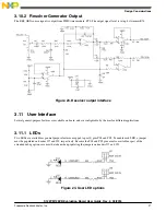
out of the VDDX node, an external ballast PNP transistor is provided on board, which is controlled by the BCTL pin.
To enable the ballast transistor, a couple of bits in register CPMUVREGCTL need to be adjusted by software (EXTXON = 1,
INTXON = 0). Additionally, a jumper needs to be placed on header J40, shorting pins 1 and 2.
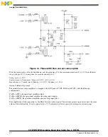
Figure 5. External ballast transistor option
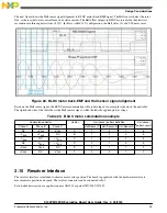
The maximum current capability of the ballast transistor will be highly dependent on the operating conditions (mainly
temperature and battery voltage). For example, the BCP53 PNP transistor on board is rated to 1.5 W at 25°C. At a nominal
battery voltage of 12 V, the estimated current capability of the transistor would be:
I = P / V, where V = (VSUP –VDDX) = 7 V
I = 1.5 W / 7 V = 214 mA
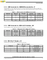
3.4 CAN/LIN Interfaces
There are two versions of the S12ZVMx12EVB board:
• S12ZVML12EVBLIN, populated with the MC9S12ZVML12 device that integrates a LIN physical layer
• S12ZVMC12EVBCAN, populated with the MC9S12ZVMC12 device that integrates a controller for a second 5 V
voltage regulator to supply an external CAN transceiver.
Design Considerations
S12ZVM12EVB Evaluation Board User Guide, Rev. 2, 03/2016
14
Freescale Semiconductor, Inc.