Board Interface Connector
MPC5777C EVB User Guide, Rev. 1
31
NXP Semiconductors
5.1.2
Daughter Card Standalone Power Input -External
A terminal power input is provided on the daughter card to enable use of the daughter card without
the motherboard.
When power is applied to the Daughter Card from Motherboard or External Terminal input or
PowerSBC with respective jumper selection, four green power LEDs adjacent to the terminal power
input connector (JP3) show the presence of the supply voltages as follows:
• LED D4 – Indicates that the 5.0 V linear regulator is enabled and working correctly
• LED D5 – Indicates that the 5.0 V switching regulator is enabled and working correctly
• LED D6 – Indicates that the 3.3 V switching regulator is enabled and working correctly
• LED D7 – Indicates that the 1.25 V switching regulator is enabled and working correctly
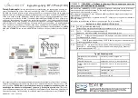
The connections of the JP7 power terminal are detailed in
Figure 21: Terminal power input connections
5.1.3
Daughter Card Standalone Power Input
–
Power SBC
Daughter Card has been designed to have onboard Power System Basis Chip (SBC),
MC33FS6522LAE
. This chip adds following options in the card,
•
SMPS Pre-regulators
•
Linear Regulators
•
SPI Interface
•
Fail Safe Output
•
RESET output to MCU (RSTB)
•
Interrupt Pulses to MCU (INTB)
•
High Speed CAN Transceiver
•
LIN Transceiver
•
Debug Mode
Power Switch SW1 should be in ON position to use Daughter card in standalone mode which enables
the use Power SBC supplies to MCU power domain.


