The SCI comprises a baud rate generator, transmitter, and receiver block. The transmitter
and receiver operate independently, although they use the same baud rate generator.
During normal operation, the MCU monitors the status of the SCI, writes the data to be
transmitted, and processes received data. The following describes each of the blocks of
the SCI.
14.4.1 Baud rate generation
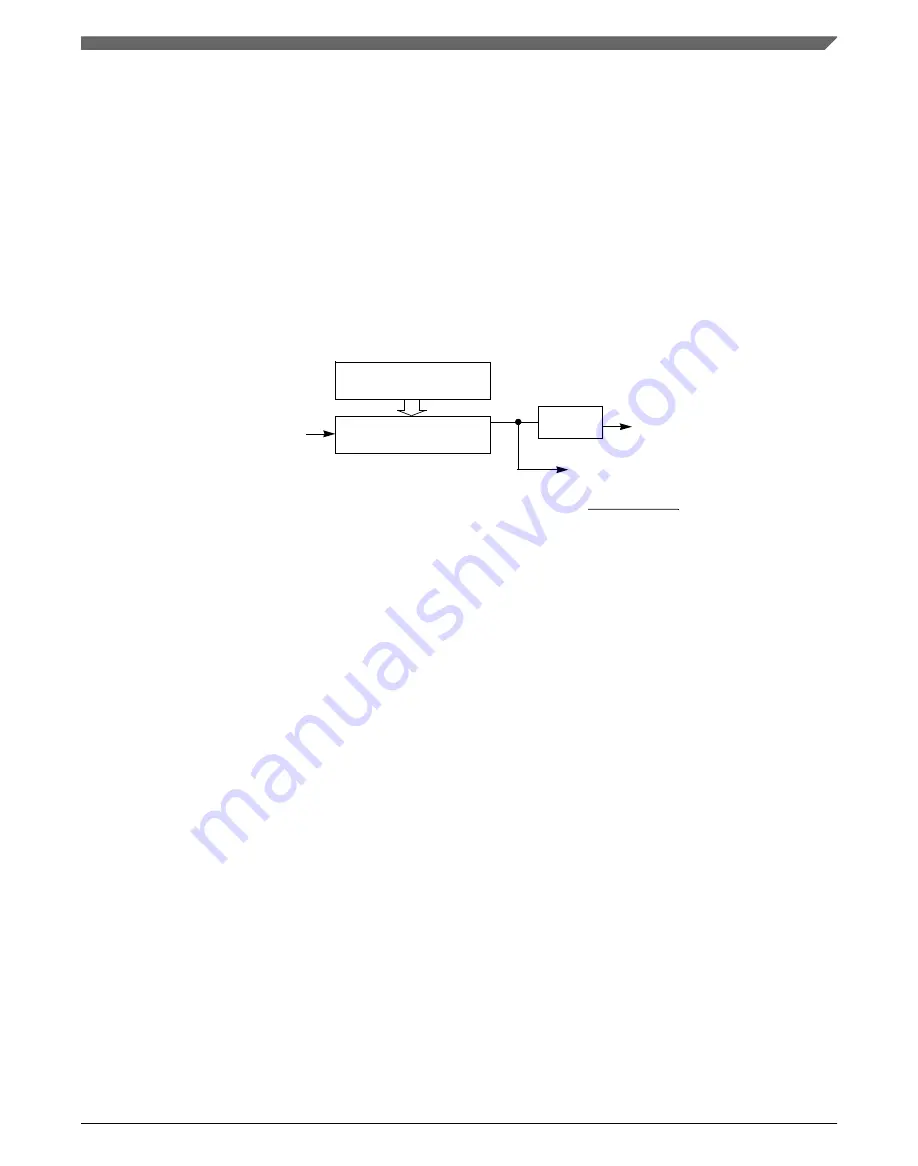
As shown in the figure found here, the clock source for the SCI baud rate generator is the
bus-rate clock.
SBR[12:0]
Baud Rate =
SBR[12:0] × 16
16
Modulo Divide By
(1 through 8191)
Baud Rate Generator
Off If [SBR12:SBR0] =0
Rx Sampling Clock
(16 × Baud Rate)
Tx Baud Rate
Divide By
16
SCI Module Clock
SCI Module Clock
Figure 14-3. SCI baud rate generation
SCI communications require the transmitter and receiver, which typically derive baud
rates from independent clock sources, to use the same baud rate. Allowed tolerance on
this baud frequency depends on the details of how the receiver synchronizes to the
leading edge of the start bit and how bit sampling is performed.
The MCU resynchronizes to bit boundaries on every high-to-low transition. In the worst
case, there are no such transitions in the full 10- or 11-bit or 12-bittime character frame
so any mismatch in baud rate is accumulated for the whole character time. For an NXP
SCI system whose bus frequency is driven by a crystal, the allowed baud rate mismatch is
about ±4.5 percent for 8-bit data format and about ±4 percent for 9-bit data format.
Although baud rate modulo divider settings do not always produce baud rates that exactly
match standard rates, it is normally possible to get within a few percent, which is
acceptable for reliable communications.
14.4.2 Transmitter functional description
This section describes the overall block diagram for the SCI transmitter, as well as
specialized functions for sending break and idle characters.
Chapter 14 Serial communications interface (SCI)
MC9S08PA4 Reference Manual, Rev. 5, 08/2017
NXP Semiconductors
283
Summary of Contents for MC9S08PA4
Page 1: ...MC9S08PA4 Reference Manual Supports MC9S08PA4 Document Number MC9S08PA4RM Rev 5 08 2017 ...
Page 2: ...MC9S08PA4 Reference Manual Rev 5 08 2017 2 NXP Semiconductors ...
Page 22: ...MC9S08PA4 Reference Manual Rev 5 08 2017 22 NXP Semiconductors ...
Page 28: ...System clock distribution MC9S08PA4 Reference Manual Rev 5 08 2017 28 NXP Semiconductors ...
Page 150: ...Port data registers MC9S08PA4 Reference Manual Rev 5 08 2017 150 NXP Semiconductors ...
Page 196: ...Human machine interfaces HMI MC9S08PA4 Reference Manual Rev 5 08 2017 196 NXP Semiconductors ...
Page 224: ...Instruction Set Summary MC9S08PA4 Reference Manual Rev 5 08 2017 224 NXP Semiconductors ...
Page 232: ...Functional Description MC9S08PA4 Reference Manual Rev 5 08 2017 232 NXP Semiconductors ...
Page 258: ...FTM Interrupts MC9S08PA4 Reference Manual Rev 5 08 2017 258 NXP Semiconductors ...
Page 294: ...Functional description MC9S08PA4 Reference Manual Rev 5 08 2017 294 NXP Semiconductors ...
Page 398: ...Resets MC9S08PA4 Reference Manual Rev 5 08 2017 398 NXP Semiconductors ...
Page 400: ...MC9S08PA4 Reference Manual Rev 5 08 2017 400 NXP Semiconductors ...