NXP Semiconductors KITFS85SKTEVM User Manual Download Page 1

UM11183

KITFS85SKTEVM evaluation board

Rev. 2.0 — 20 February 2019

User guide

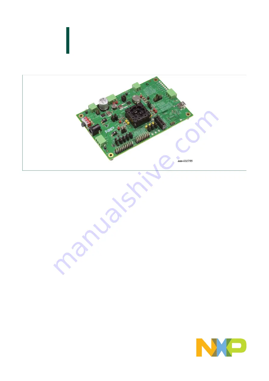
Figure 1. KITFS85SKTEVM

Important Notice

NXP provides the enclosed product(s) under the following conditions:
This evaluation kit is intended for use of ENGINEERING DEVELOPMENT OR EVALUATION PURPOSES ONLY. It is provided as a

sample IC pre-soldered to a printed circuit board to make it easier to access inputs, outputs, and supply terminals. This evaluation board

may be used with any development system or other source of I/O signals by simply connecting it to the host MCU or computer board via

off-the-shelf cables. This evaluation board is not a Reference Design and is not intended to represent a final design recommendation for

any particular application. Final device in an application will be heavily dependent on proper printed circuit board layout and heat sinking

design as well as attention to supply filtering, transient suppression, and I/O signal quality.
The goods provided may not be complete in terms of required design, marketing, and or manufacturing related protective considerations,

including product safety measures typically found in the end product incorporating the goods. Due to the open construction of the product,

it is the user's responsibility to take any and all appropriate precautions with regard to electrostatic discharge. In order to minimize risks

associated with the customers applications, adequate design and operating safeguards must be provided by the customer to minimize

inherent or procedural hazards. For any safety concerns, contact NXP sales and technical support services.
Should this evaluation kit not meet the specifications indicated in the kit, it may be returned within 30 days from the date of delivery and will

be replaced by a new kit.
NXP reserves the right to make changes without further notice to any products herein. NXP makes no warranty, representation or

guarantee regarding the suitability of its products for any particular purpose, nor does NXP assume any liability arising out of the

application or use of any product or circuit, and specifically disclaims any and all liability, including without limitation consequential or

incidental damages. Typical parameters can and do vary in different applications and actual performance may vary over time. All operating

parameters, including Typical, must be validated for each customer application by customer’s technical experts.
NXP does not convey any license under its patent rights nor the rights of others. NXP products are not designed, intended, or authorized

for use as components in systems intended for surgical implant into the body, or other applications intended to support or sustain life, or

for any other application in which the failure of the NXP product could create a situation where personal injury or death may occur.
Should the Buyer purchase or use NXP products for any such unintended or unauthorized application, the Buyer shall indemnify and hold 

NXP and its officers, employees, subsidiaries, affiliates, and distributors harmless against all claims, costs, damages, and expenses, and

reasonable attorney fees arising out of, directly or indirectly, any claim of personal injury or death associated with such unintended or

unauthorized use, even if such claim alleges NXP was negligent regarding the design or manufacture of the part.

Summary of Contents for KITFS85SKTEVM

Page 1: ...technical support services Should this evaluation kit not meet the specifications indicated in the kit it may be returned within 30 days from the date of delivery and will be replaced by a new kit NXP...

Page 2: ...a good flexibility This board supports FS84 FS85 family of devices 2 Finding kit resources and information on the NXP web site NXP Semiconductors provides online resources for this evaluation board a...

Page 3: ...e FlexGUI software allows access to the registers in read and write mode All regulators are accessible through connectors Nonuser signals like DC DC switcher node are mapped on test points Digital sig...

Page 4: ...gnal or regulator status Support OTP fuse capabilities USB connection for register access OTP emulation and programming Voltage monitoring jumper setting Note Due to the socket all current capabilitie...

Page 5: ...k R180 27 4 k BUCK3_MON3 BUCK3 VMON_08V J24 1 2 3 GND HDR 1X3 R189 22 1 k R178 68 1 k LDO_MON4 LDO1 VMON_08V J21 1 2 3 GND HDR 1X3 R192 22 1 k R182 68 1 k LDO2 GND R208 22 1 k R207 115 k Figure 2 VMO...

Page 6: ...R145 0 DNP Figure 4 BUCK1 and BUCK2 multiphase configuration 4 1 5 SPI I2C The SPI and I2C buses are connected to KL25Z MCU The user can use either one or the other The choice can be done at start of...

Page 7: ...ovided to feed VDDI2C This LDO can also be used to feed VDDIO which is the default implementation The I2C is compatible with 1 8 V or 3 3 V while VDDIO is compatible with 3 3 V and 5 0 V For this reas...

Page 8: ...hree times using mirror registers The user can first load the mirror register content with the desired contents then decide either to use the device in Emulation mode or to burn the next sector The fi...

Page 9: ...VSUP_UVH WAKE12VIH SPI I2C OTP pgm OFF PWR UP ON SPI I2C Figure 10 Debug mode entry Figure 11 shows the hardware kit implementation aaa 032762 SW1 SW2 VSUP1 2 FS8500 Debug ref OTP level DBG 8 V 2 1 3...

Page 10: ...ng voltage switch 12 VBOOST and BUCK3 power supply 13 DEBUG voltage source 14 Compensation network selection 15 VDDIO selection 16 SPI RSTb FS0b connection to MCU 17 RSTb INTb and FS0b signals 18 VMON...

Page 11: ...m FS84 fit for ASIL B and FS85 fit for ASIL D pin to pin and software compatible The FS85 FS84 is an automotive functionally safe multi output power supply integrated circuit with focus on Radar Visio...

Page 12: ...frequency tuning 2x linear voltage regulators for MCU IOs and ADC supply external physical layer Configurable output voltage and current capability up to 400 mA DC Standby OFF mode with very low sleep...

Page 13: ...G 8 0 V Blue DBG pin voltage 8 0 V OTP programming D13 RSTb Red RSTb asserted logic level 0 D14 INTb Red INTb asserted logic level 0 D15 FS0b Red FS0b asserted logic level 0 D16 P3V3_KL25 Green P3V3_K...

Page 14: ...Table 7 LDO1 LDO2 connector J2 Schematic label Signal name Description J2 1 LDO1 LDO1 power supply output J2 2 LDO2 LDO2 power supply output J2 3 GND Ground Table 8 VPRE connector J3 Schematic label...

Page 15: ...nit 2 J29 20 GND Ground 4 3 3 4 Program connector J30 Table 10 Program connector J30 Schematic label Signal name Description J30 1 WAKE1 WAKE1 input J30 2 MOSI SPI master output slave input J30 3 VDDI...

Page 16: ...e Description TP1 GND Ground TP2 GND Ground TP3 LDO2 LDO2 regulator output TP4 LDO1 LDO1 regulator output TP5 VPRE VPRE DC DC regulator output TP6 GND Ground TP7 VBOOST VBOOST DC DC output TP8 BOOST_L...

Page 17: ...P shunt 3 4 For current measurement insert amperemeter 1 2 BUCK_INQ tied to VPRE J8 BUCK3 input 2 3 BUCK_INQ tied to VBOOST 1 2 LDO1_IN connected to VPRE J9 LDO1 input 2 3 LDO1_IN connected to VBOOST...

Page 18: ...V J24 VMON3 2 3 VMON3 tied to BUCK3 J25 RSTb 1 2 Reset LED Enabled when jumper is plugged J26 INTb 1 2 Interrupt LED Enabled when jumper is plugged J27 FS0b 1 2 FS0b LED Enabled when jumper is plugged...

Page 19: ...the Windows PC workstation consists of three steps 1 Install the appropriate Java SE Runtime Environment JRE 2 Install Windows 7 FlexGUI driver 3 Install FlexGUI software package 5 1 Installing the J...

Page 20: ...evaluation board UM11183 All information provided in this document is subject to legal disclaimers NXP B V 2019 All rights reserved User guide Rev 2 0 20 February 2019 20 50 4 In the SECON FLEX GUI SL...

Page 21: ...n board UM11183 All information provided in this document is subject to legal disclaimers NXP B V 2019 All rights reserved User guide Rev 2 0 20 February 2019 21 50 5 in the Update Software Driver win...

Page 22: ...ed in this document is subject to legal disclaimers NXP B V 2019 All rights reserved User guide Rev 2 0 20 February 2019 22 50 6 Select Let me pick from a list of device drivers on my computer and the...

Page 23: ...oard UM11183 All information provided in this document is subject to legal disclaimers NXP B V 2019 All rights reserved User guide Rev 2 0 20 February 2019 23 50 9 Click Browse 10 In the Locate File w...

Page 24: ...ormation provided in this document is subject to legal disclaimers NXP B V 2019 All rights reserved User guide Rev 2 0 20 February 2019 24 50 11 In the Install from Disk window click OK 12 If prompted...

Page 25: ...d in this document is subject to legal disclaimers NXP B V 2019 All rights reserved User guide Rev 2 0 20 February 2019 25 50 13 Close the window when the installation is complete 14 In the Virtual Co...

Page 26: ...TEVM evaluation board UM11183 All information provided in this document is subject to legal disclaimers NXP B V 2019 All rights reserved User guide Rev 2 0 20 February 2019 26 50 The Virtual Com Port...

Page 27: ...nstalling FlexGUI software package The FlexGUI software installation requires only extracting the zip file in a desired location 1 If necessary install the Java JRE and Windows 7 FlexGUI driver 2 Down...

Page 28: ...er Configuration J17 connect 1 2 connect 5 0 V on DBG pin from the USB 2 Configure switches for the configuration Table 17 Switch configuration Switch Configuration SW1 middle position VBAT off SW2 op...

Page 29: ...he DBG pin level Normal mode is set by tying DBG to ground Debug mode is set by setting DBG voltage to 5 0 V In OTP emulation you can overwrite the mirror registers from a given OTP fuse configuration...

Page 30: ...0 50 Figure 20 OTP_conf_failsafe_reg spreadsheet example 3 See the OTP_conf_summary sheet to review the complete configuration main and fail safe Figure 21 OTP_conf_summary example 4 Generate the scri...

Page 31: ...ile in Debug mode all regulators are turned Off 4 Load the mirror registers to work in OTP emulation mode See Section 8 3 Working with the Script editor 5 Unplug jumper J17 1 2 to start the device wit...

Page 32: ...T of FS_WD_WINDOW 3 FS_I_SAFE_INPUTS 0x51C6 FCCU_CFG 1 0 0x0 0x1 Monitoring by pair FCCU12_FLT_POL 0 1 FCCU1 or 2 0 is a fault 4 FS_I_NOT_SAFE_INPUTS 0xAC18 NOT of FS_I_SAFE_INPUTS 5 FS_WD_ANSWER 0x5A...

Page 33: ...the FlexGUI application After FlexGUI is launched with the flexgui app bat file the FlexGUI launcher displays available kits Communication bus SPI or I2C can be selected at this level It is also poss...

Page 34: ...t This change is managed by the onboard MCU to communicate with the desired bus It is also possible to change the clock frequency using this panel Note that in the case of I2C most of the time the def...

Page 35: ...on that Poll button is enabled 8 3 Working with the Script editor The register and OTP emulation can be configured with the script editor This is particularly useful to try various OTP configurations...

Page 36: ...6 50 8 3 1 Script text editor Using Script editor you can execute any command either directly or from a file It is also possible to save and modify a script Using the brush symbol it is possible to cl...

Page 37: ...ers NXP B V 2019 All rights reserved User guide Rev 2 0 20 February 2019 37 50 Figure 27 Build a command The value 0x0800 is sent to the register M_REG_CTRL1 BUCK2DIS The user can then send it to the...

Page 38: ..._I_NOT_SAFE_INPUTS AC18 SET_REG FS85 safety FS_WD_ANSWER 0x5AB2 SET_REG FS85 safety FS_STATES 0x4000 SET_REG FS85 safety FS_WD_ANSWER 0x5AB2 SET_REG FS85 safety FS_WD_ANSWER 0x5AB2 SET_REG FS85 safety...

Page 39: ...igure 31 Register map Register map allows access to functional register safety register and write init register which are accessible only during initialization phase Read allows you to read any regist...

Page 40: ...frequencies and spread spectrum 8 4 3 Regulators The regulator has two main areas Low voltage LV regulators configuration VPRE compensation network calculation Each regulator can either be enabled or...

Page 41: ...ided in this document is subject to legal disclaimers NXP B V 2019 All rights reserved User guide Rev 2 0 20 February 2019 41 50 Figure 34 Measurements 8 4 5 Interrupt flags This tab allows you to set...

Page 42: ...sters that can be configured to close the initialization phase Note that the initialization phase is closed by the first good watchdog refresh before 256 ms timeout Figure 36 INIT safety 8 4 7 Diag sa...

Page 43: ...ary 2019 43 50 Figure 37 Diag safety The FS_Release_FS0b command calculates and sends the right secure16 bit word to release FS0b A simplified way to release FS0b after power up is to first select the...

Page 44: ...en turns Off Note that the blue LED on the board indicates that an 8 0 V voltage is available on the Debug pin This voltage is used only during the burning process and should not be applied in any oth...

Page 45: ...n is read from mirror register It is possible to modify it and update the mirror register As an example the slot sequence is filled at start up with the content of OTP fuses Then the user can decide t...

Page 46: ...laimers NXP B V 2019 All rights reserved User guide Rev 2 0 20 February 2019 46 50 8 4 10 TestMode Mirrors_Main and TestMode Mirrors_Failsafe The TestModeMirrors_Main and TestModeMirrors_FailSafe tabs...

Page 47: ...documentation downloads and software and tools http www nxp com KITFS85SKTEVM 2 FS8500 product information on FS8500 Safety system basis chip for S32 microcontrollers fit for ASIL D http www nxp com F...

Page 48: ...s applications or products or the application or use by customer s third party customer s Customer is responsible for doing all necessary testing for the customer s applications and products using NXP...

Page 49: ...g 5 SPI connection to KL25Z 6 Fig 6 J30 SPI connection 7 Fig 7 VDDIO selection 7 Fig 8 VDDI2C supply 7 Fig 9 OTP configuration 8 Fig 10 Debug mode entry 9 Fig 11 OTP hardware implementation 9 Fig 12 E...

Page 50: ...Indicators 12 4 3 3 Connectors 13 4 3 3 1 VBAT connector J1 13 4 3 3 2 Output power supply connectors 14 4 3 3 3 Debug connector J29 14 4 3 3 4 Program connector J30 15 4 3 4 Test points 15 4 3 5 Jum...

Reviews: