


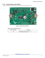

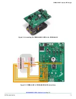

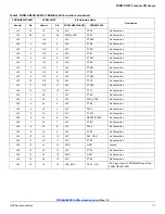


FRDM-KL25Z Freedom SPI dongle
FRDM-HB2001-EVM evaluation board
, Rev. 1.0
16
NXP Semiconductors
Table 9. FRDM-HB2001-EVM to FRDM-KL25Z Connections
FRDM-HB2001-EVM
FRDM-KL25Z
Pin Hardware Name
Description
Header
Pin
Header
Pin
FRDM-HB2001-EVM
FRDM-KL25Z
J24
1
J1
1
N/C
PTC7
No Connection
J24
2
J1
2
N/C
PTA1
No Connection
J24
3
J1
3
N/C
PTC0
No Connection
J24
4
J1
4
N/C
PTA2
No Connection
J24
5
J1
5
N/C
PTC3
No Connection
J24
6
J1
6
N/C
PTD4
No Connection
J24
7
J1
7
N/C
PTC4
No Connection
J24
8
J1
8
N/C
PTA12
No Connection
J24
9
J1
9
N/C
PTC5
No Connection
J24
10
J1
10
N/C
PTA4
No Connection
J24
11
J1
11
N/C
PTC6
No Connection
J24
12
J1
12
N/C
PTA5
No Connection
J24
13
J1
13
N/C
PTC10
Not Connected
J24
14
J1
14
N/C
PTC8
No Connection
J24
15
J1
15
N/C
PTC11
Not Connected
J24
16
J1
16
N/C
PTC9
No Connection
J10
1
J2
1
DATA0/IN1
PTC12
IN1 signal for the H-Bridge
J10
2
J2
2
N/C
PTA13
No Connection
J10
3
J2
3
DATA1/IN2
PTC13
IN2 signal for the H-Bridge
J10
4
J2
4
N/C
PTD5
No Connection
J10
5
J2
5
FS_B
PTC16
Fault status pin to report fault
J10
6
J2
6
CS_B
PTD0
Chip select bar pin
J10
7
J2
7
N/C
PTC17
No Connection
J10
8
J2
8
MOSI
PTD2
Master output serial input
J10
9
J2
9
N/C
PTA16
No Connection
J10
10
J2
10
MISO
PTD3
Master input serial output
J10
11
J2
11
N/C
PTA17
No Connection
J10
12
J2
12
SCLK
PTD1
Clock for SPI
J10
13
J2
13
N/C
PTE31
No Connection
J10
14
J2
14
GND
GND
No Connection
J10
15
J2
15
N/C
N/C
No Connection
J10
16
J2
16
N/C
VREFH
No Connection
J10
17
J2
17
CFB_READ
PTD6
ADC input for monitoring the CFB pin
J10
18
J2
18
N/C
PTE0
Disable signal to tri-state the output and put
the part in Sleep mode (Active Low)