


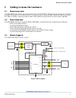


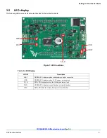


Getting to know the hardware
FRDM-HB2001-EVM evaluation board
, Rev. 1.0
10
NXP Semiconductors
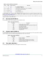
3.6
Jumper definitions
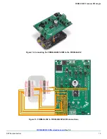
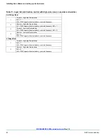
The
illustrates the evaluation board jumper locations.
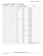
explains the function of each position. Blue fonts in the Jumper
Position column indicate the default settings for use with the FRDM-KL25Z.
Figure 8. Jumper locations
Table 4. Jumper definitions
Name
Signal
Jumper Position
Connection
J1
IN1
1–2
IN1 control through MCU parallel output on J10 Pin 1 (DATA0)
2–3
IN1 control through external input on J15 Pin 1
J2
DIS
1–2
DIS control through MCU parallel output on J10 Pin 13 (CTRL1)
2–3
DIS connected to GND to keep the outputs enabled
J3
IN2
1–2
IN2 control through MCU parallel output on J10 Pin 3 (DATA1)
2–3
IN2 control through external input on J15 Pin 2
J4
CS_B
1–2
CS_B control through MCU SPI output J10 Pin 6 (SPI_CS_B)
2–3
CS_B pulled up to V
DD
for operation without SPI
J5
ENBL
1–2
ENBL control through MCU parallel output J10 Pin 11 (CTRL0)
2–3
ENBL pulled up to V
DD
to keep the outputs enabled
J6
SCLK
1–2
SPI clock SCLK from MCU J10 Pin 12 (SPI_SCLK
2–3
SCLK connected to GND for operation without SPI
J7
MOSI
1–2
MOSI control through MCU SPI output J10 Pin 8 (SPI_MOSI)
2–3
MOSI connected to GND for operation without SPI
J8
MISO
1–2
MISO control through MCU SPI output J10 Pin 10 (SPI_MISO)
2–3
MISO not connected for operation without SPI
J11
CFB
1-2
CFB connected to 200
resistor
J14
VDDQ
1–2
VDD connected to VDDQ
2–3
VDDQ not connected
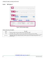
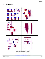
DIS
VDD
CFB
ENBL
IN2
IN1
EX_IN
CFB_R
VDD_REG
MOSI
SCLK
MISO
CS_B
VDDQ
FS_B