After Sales
Technical Documentation
RAE/RAK–1N
UIF
Page 4– 7
Amendment 1 04/97
Both flexes are made of flexible material. Flexible material is needed
because the hinge will be opened thousands of times and the signals
must be working all the time.
UIF Electronics
The following sections of circuitry are on the UIF module:
– CMT LCD Display Module
– CMT LCD voltage divider & temperature compensation circuit.
– CMT Keypad & CMT LCD illuminating circuits.
– CMT & Soft keypad matrix.
– Antenna impedance matching circuit.
– Hinge flex connector.
– PDALCD flex connector.
Technical Specification
UIF Electrical Characteristics
DC Characteristics
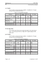
Table 1. Supply Voltages and Power Consumption
Pin / Conn.
Line Symbol
Minimum
Typical /
Nominal
Maximum
Unit / Notes
2/X001
VL1
4.65
4.8
4.95
V
1.5 mA
LCD material B
0.8 mA
LCD material D
(without tempera-
ture compensation)
1/X001
VBATT
5.3
7.2
8.4
V
40 mA
Display illumination
40 mA
Keypad illumination
27/X001
LCDVCC
3.3V
PDALCD Logic
voltage
28/X001
LCDVEE
17V
22V
25V
PDALCD LCD volt-
age
Summary of Contents for 9000i
Page 7: ...After Sales Technical Documentation RAE RAK 1N Series Original 08 96 Chapter 1 Overview ...
Page 287: ...After Sales Technical Documentation RAE RAK 1N Series Original 08 96 Chapter 9 Service Tools ...
Page 301: ...After Sales Technical Documentation RAE 1N Series Original 04 97 Chapter 10 Schematics ...
Page 303: ...RAE 1N Original 08 96 10 11 Page 1 Figure 1 Component Layout Bottom ...
Page 304: ...RAE 1N Original 08 96 10 12 Page Figure 2 Component Layout Top ...
Page 305: ...RAE 1N Original 08 96 10 13 Page Figure 3 Baseband Circuit Diagram PWRU ...
Page 306: ...RAE 1N Original 08 96 10 14 Page Figure 4 Baseband Circuit Diagram MCM1 ...
Page 307: ...RAE 1N Original 08 96 10 15 Page Figure 5 Baseband Circuit Diagram MCM2 ...
Page 308: ...RAE 1N Original 08 96 10 16 Page Figure 6 RF TX Circuit Diagram ...
Page 309: ...RAE 1N Original 08 96 10 17 Page Figure 7 RF RX Circuit Diagram ...
Page 310: ...RAK 1N 10 20 Page Amendment 1 04 97 Figure 18 PCN Component Layout Bottom ...
Page 311: ...RAK 1N 10 21 Page Amendment 1 04 97 Figure 19 PCN Component Layout Top ...
Page 312: ...RAK 1N 10 22 Page Amendment 1 04 97 Figure 20 PCN RF TX ...
Page 313: ...RAK 1N 10 23 Page Amendment 1 04 97 Figure 21 PCN RF RX ...
Page 314: ...RAK 1N 10 24 Page Amendment 1 04 97 Figure 22 UIF Schematic PCN ...
Page 315: ...RAK 1N 10 25 Page Amendment 1 04 97 Figure 23 UIF Component Layout PCN ...
Page 316: ...RAE 1N Original 05 97 10 3 Page Figure 1 PDA Block Diagram Edit 82 for layout 13a ...
Page 317: ...RAE 1N Original 05 97 10 4 Page Figure 2 PDA Power Unit PWRU Edit 108 for layout 13a ...
Page 318: ...RAE 1N Original 05 97 10 5 Page Figure 3 PDA Serial Interface SIRU Edit 24 for layout 13a ...
Page 319: ...RAE 1N Original 05 97 10 6 Page Figure 4 PDA MCU and Memory PROCU Edit 121 for layout 13a ...
Page 320: ...RAE 1N Original 05 97 10 7 Page Figure 5 PDA EMIU Edit 21 for layout 13a ...
Page 321: ...RAE 1N Original 05 97 10 8 Page Figure 6 Keyboard matrix Edit 24 for layout 13a ...
Page 322: ...RAE 1N Original 05 97 10 9 Page Figure 7 PDA Memory Edit 28 for layout 13a ...
Page 323: ...RAE 1N Original 05 97 10 10 Page Figure 8 PDA Component Layout 13a ...
Page 324: ...RAE 1N Original 08 96 10 18 Page Figure 1 UIF Schematic ...
Page 325: ...RAE 1N Original 08 96 10 19 Page Figure 2 Component Layout Uif ...
Page 326: ...After Sales Technical Documentation RAE RAK 1N Series Original 08 96 Accessories ...
Page 352: ...After Sales Technical Documentation Appendix 2 RAE RAK 1N Amendment 1 04 97 PARTS LISTS ...
Page 402: ...After Sales Technical Documentation Appendix 1 RAE RAK 1N Original 08 96 QUICK GUIDE ...
Page 434: ......


