background image

CHAPTER 4   INTERNAL CPU FUNCTION

64

User’s Manual  U10676EJ3V0UM

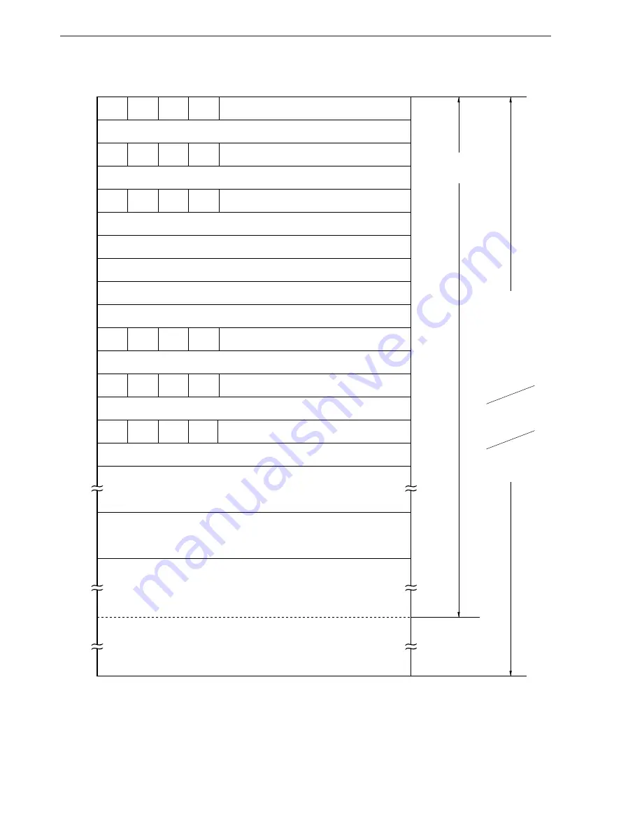
Figure 4-3.  Program Memory Map

7

6

0

MBE

RBE

Internal reset start address

(higher 4 bits)

Internal reset start address

(lower 8 bits)

MBE

RBE

INTBT start address

(higher 4 bits)

INTBT start address

(lower 8 bits)

MBE

RBE

INT0 start address

(higher 4 bits)

INT0 start address

(lower 8 bits)

MBE

RBE

INTT0 start address

(higher 4 bits)

INTT0 start address

(lower 8 bits)

MBE

RBE

INTT1/INTT2 start address

(higher 4 bits)

INTT1/INTT2 start address

(lower 8 bits)

MBE

RBE

INTEE start address

(higher 4 bits)

INTEE start address

(lower 8 bits)

GET instruction reference table

0000H

0001H

0002H

0003H

0004H

0005H

0006H

0007H

0008H

0009H

000AH

000BH

000CH

000DH

000EH

000FH

0020H

007FH

0080H

07FFH

0800H

0FFFH

CALLF !faddr instruction

entry address

Branch address of

BR !addr

BRCB !caddr

BR BCDE
BR BCXA

BRA !addr1

Note

CALL !addr

CALLA !addr1

Note

instructions

GETI Branch/call

Addresses

BR $addr instruction

relative branch address

(–15 to –1, +2 to +16)

Address

5

0

0

0

0

0

0

4

0

0

0

0

0

0

Note

Can be used in the MkII mode only.

Remark

In addition to the above, a branch can be made to an address with the lower 8-bits only of the PC changed

by means of a BR PCDE or BR PCXA instruction.

Summary of Contents for PD754144

Page 1: ...User s Manual Printed in Japan µPD754144 754244 4 Bit Single Chip Microcontrollers µPD754144 µPD754244 Document No U10676EJ3V0UM00 3rd edition Date Published November 2002 N CP K 1997 ...

Page 2: ...2 User s Manual U10676EJ3V0UM MEMO ...

Page 3: ...be touched with bare hands Similar precautions need to be taken for PW boards with semiconductor devices on it 2 HANDLING OF UNUSED INPUT PINS FOR CMOS Note No connection for CMOS device inputs can be cause of malfunction If no connection is provided to the input pins it is possible that an internal input level may be generated due to noise etc hence causing malfunction CMOS devices behave differe...

Page 4: ... safety of NEC Electronics products customers agree and acknowledge that the possibility of defects thereof cannot be eliminated entirely To minimize risks of damage to property or injury including death to persons arising from defects in NEC Electronics products customers must incorporate sufficient safety measures in their design such as redundancy fire containment and anti failure features NEC ...

Page 5: ...1 6841 1138 Fax 021 6841 1137 NEC Electronics Taiwan Ltd Taipei Taiwan Tel 02 2719 2377 Fax 02 2719 5951 NEC Electronics Singapore Pte Ltd Novena Square Singapore Tel 6253 8311 Fax 6250 3583 J02 11 NEC Electronics Europe GmbH Duesseldorf Germany Tel 0211 65 03 01 Fax 0211 65 03 327 Sucursal en España Madrid Spain Tel 091 504 27 87 Fax 091 504 28 60 Vélizy Villacoublay France Tel 01 30 67 58 00 Fax...

Page 6: ... during interrupt service INTBT has higher priority and INTT0 and INTT2 have lower priority p 253 Correction of instruction code of BR BCDE in 11 3 Opcode of Each Instruction p 296 Deletion of flash related products in configuration diagram in APPENDIX A DEVELOPMENT TOOLS p 297 in 2nd edition Deletion of APPENDIX A LIST OF FUNCTIONS OF µPD754144 754244 AND 75F4264 The mark shows major revised poin...

Page 7: ... use this manual as a manual for µPD754144 RC oscillation fCC Unless otherwise specified the µPD754244 crystal ceramic oscillation fX is treated as the representative model in this manual Check the functional differences between the µPD754144 and µPD754244 by referring to 1 3 Differences Between µPD754144 and 754244 and take the µPD754244 as µPD754144 and fX as fCC To check the functions of an ins...

Page 8: ...sor U12598E Documents related to development tools hardware user s manuals Document Name Document No IE 75000 R IE 75001 R In Circuit Emulator EEU 1455 IE 75300 R EM Emulation Board U11354E EP 754144GS R Emulation Probe U10695E Other documents Document Name Document No SEMICONDUCTOR SELECTION GUIDE Products Packages X13769E Semiconductor Device Mounting Technology Manual C10535E Quality Grades on ...

Page 9: ...754244 only 28 2 2 11 RESET 28 2 2 12 IC 29 2 2 13 VDD 29 2 2 14 VSS 29 2 3 Pin I O Circuits 30 2 4 Processing of Unused Pins 31 CHAPTER 3 FEATURES OF ARCHITECTURE AND MEMORY MAP 32 3 1 Bank Configuration of Data Memory and Addressing Modes 32 3 1 1 Bank configuration of data memory 32 3 1 2 Addressing mode of data memory 34 3 2 Bank Configuration of General Purpose Registers 45 3 3 Memory Mapped ...

Page 10: ...2 Clock Generator 103 6 2 1 Configuration of clock generator 103 6 2 2 Function and operation of clock generator 105 6 2 3 Setting CPU clock 112 6 3 Basic Interval Timer Watchdog Timer 114 6 3 1 Configuration of basic interval timer watchdog timer 114 6 3 2 Basic interval timer mode register BTM 115 6 3 3 Watchdog timer enable flag WDTM 117 6 3 4 Operation as basic interval timer 118 6 3 5 Operati...

Page 11: ...Reset Function 227 9 2 Watchdog Flag WDF Key Return Flag KRF 231 CHAPTER 10 MASK OPTIONS 233 10 1 Pin Mask Options 233 10 1 1 Mask option of P70 KR4 to P73 KR7 233 10 1 2 RESET pin mask option 233 10 2 Oscillation Stabilization Wait Time Mask Option 233 CHAPTER 11 INSTRUCTION SET 234 11 1 Unique Instructions 234 11 1 1 GETI instruction 234 11 1 2 Bit manipulation instruction 235 11 1 3 String effe...

Page 12: ...287 11 4 13 Input output instructions 288 11 4 14 CPU control instruction 289 11 4 15 Special instructions 290 APPENDIX A DEVELOPMENT TOOLS 293 APPENDIX B ORDERING MASK ROM 297 APPENDIX C INSTRUCTION INDEX 298 C 1 Instruction Index By Function 298 C 2 Instruction Index Alphabetical Order 301 APPENDIX D HARDWARE INDEX 304 APPENDIX E REVISION HISTORY 306 ...

Page 13: ...e 72 4 11 Data Saved to Stack Memory MkII Mode 73 4 12 Data Restored from Stack Memory MkII Mode 73 4 13 Configuration of Program Status Word 74 4 14 Configuration of Bank Select Register 78 5 1 Format of EEPROM Write Control Register 81 5 2 EEPROM Write Control Register in EEPROM Read Manipulation 84 5 3 EEPROM Write Control Register in EEPROM Write Manipulation 85 6 1 Data Memory Address of Digi...

Page 14: ... 6 36 Setting of Timer Counter Mode Register 146 6 37 Setting of Timer Counter Control Register 147 6 38 PWM Pulse Generator Operating Configuration 149 6 39 PWM Pulse Generator Operating Timing 149 6 40 Setting of Timer Counter Mode Registers 152 6 41 Setting of Timer Counter Control Register 153 6 42 Configuration When Timer Counter Operates 157 6 43 Timing of Count Operation 158 6 44 Setting of...

Page 15: ...3 7 11 Format of INT2 Edge Detection Mode Register IM2 214 8 1 Releasing Standby Mode 218 8 2 Wait Time After Releasing STOP Mode 220 8 3 STOP Mode Release by Key Return Reset or RESET Input 221 9 1 Configuration of Reset Circuit 227 9 2 Reset Operation by RESET Signal 228 9 3 WDF Operation in Generating Each Signal 231 9 4 KRF Operation in Generating Each Signal 232 ...

Page 16: ...atures of Digital Ports 89 6 2 I O Pin Manipulation Instructions 97 6 3 Operation When I O Port Is Manipulated 99 6 4 Specifying Connection of Pull up Resistor 100 6 5 Maximum Time Required for CPU Clock Switching 112 6 6 Mode List 122 6 7 Resolution and Longest Set Time 8 Bit Timer Counter Mode 139 6 8 Resolution and Longest Set Time 16 Bit Timer Counter Mode 154 7 1 Types of Interrupt Sources 18...

Page 17: ... operation on chip Variable instruction execution time useful for high speed operation and power saving µPD754144 RC oscillator resistors and capacitors are externally provided 4 8 16 64 µs at fCC 1 0 MHz µPD754244 Crystal ceramic oscillator 0 95 µs 1 91 µs 3 81 µs 15 3 µs at fX 4 19 MHz 0 67 µs 1 33 µs 2 67 µs 10 7 µs at fX 6 0 MHz Four timer channels Key return reset function for key less entry ...

Page 18: ...peration 8 4 banks 8 bit operation 4 4 banks I O ports CMOS input 4 Pull up resistors can be incorporated by mask option CMOS I O 9 On chip pull up resistors can be specified by software Total 13 Timers 4 channels 8 bit timer counter 3 channels can be used as 16 bit timer counter Basic interval watchdog timer 1 channel Programmable threshold port 2 channels Bit sequential buffer 16 bits Vectored i...

Page 19: ...ction execution time 4 8 16 64 µs at fCC 1 0 MHz 0 95 1 91 3 81 15 3 µs at fX 4 19 MHz 0 67 1 33 2 67 10 7 µs at fX 6 0 MHz System clock oscillator RC oscillator Crystal ceramic oscillator resistors and capacitors are externally provided Startup time after reset Fixed to 56 µs at 1 MHz Can be selected by mask option from the following two 217 fX 31 3 ms at 4 19 MHz 21 8 ms at 6 0 MHz 215 fX 7 81 m...

Page 20: ...T2 PTO0 P30 PTO1 P31 PTO2 P32 INT0 P61 KRREN KR4 P70 KR7 P73 AVREF P60 PTH00 P62 PTH01 P63 ALU Program counter Program memory ROM 4096 8 bits Decode and control CY SP 8 SBS Bank General reg Data memory RAM 128 4 bits EEPROM 16 8 bits Port 3 4 Port 6 4 Port 7 4 Port 8 Bit seq buffer 16 P30 to P33 P60 to P63 P70 to P73 P80 Clock divider System clock generator Standby control fX 2N φ CPU clock IC VDD...

Page 21: ...astic SOP 7 62 mm 300 µPD754144GS BA5 20 pin plastic SSOP 7 62 mm 300 µPD754144GS GJG 1 2 3 4 5 6 7 8 9 10 20 19 18 17 16 15 14 13 12 11 RESET CL1 CL2 VSS IC VDD P60 AVREF P61 INT0 P62 PTH00 P63 PTH01 KRREN P80 P30 PTO0 P31 PTO1 P32 PTO2 P33 P70 KR4 P71 KR5 P72 KR6 P73 KR7 IC Internally Connected Directly connect to VDD ...

Page 22: ... mm 300 µPD754244GS BA5 20 pin plastic SSOP 7 62 mm 300 µPD754244GS GJG IC Internally Connected Directly connect to VDD 1 2 3 4 5 6 7 8 9 10 20 19 18 17 16 15 14 13 12 11 RESET X1 X2 VSS IC VDD P60 AVREF P61 INT0 P62 PTH00 P63 PTH01 KRREN P80 P30 PTO0 P31 PTO1 P32 PTO2 P33 P70 KR4 P71 KR5 P72 KR6 P73 KR7 ...

Page 23: ...Key return 4 to 7 INT0 External vectored interrupt 0 PTH00 PTH01 Programmable threshold port analog input 0 1 PTO0 to PTO2 Programmable timer output 0 to 2 KRREN Key return reset enable CL1 CL2 RC oscillator X1 X2 Crystal ceramic oscillator IC Internally connected RESET Reset AVREF Analog reference VSS Ground VDD Positive power supply ...

Page 24: ...tt triggered input 2 Do not specify connection of an on chip pull up resistor when using a programmable threshold port Programmable 4 bit I O port Port 3 Input output can be specified in 1 bit units On chip pull up resistor can be specified by software in 4 bit units Programmable 4 bit I O port Port 6 Input output can be specified in 1 bit units An on chip pull up resistor can be specified by soft...

Page 25: ...return reset enable pin Input B Reset signal is generated at falling edge of KRn when KRREN high in STOP mode AVREF Input P60 Reference voltage input pin Input F A CL1 Input Provided in µPD754144 only These pins connect R and C for system clock CL2 Output oscillation No external clock can be input to these pins X1 Input Provided in µPD754244 only These pins connect crystal ceramic oscillator for X...

Page 26: ...d POGB Specify connection of the pull up resistor to ports 3 and 6 in 4 bit units Connection of the pull up resistor to port 8 can be specified in 1 bit units I O for ports 3 and 6 is possible in 4 bit or 1 bit units Manipulation in 8 bit units is not possible Generation of the RESET signal sets the input mode 2 2 2 P70 to P73 Port 7 input pins shared with KR4 to KR7 Port 7 is a 4 bit input port T...

Page 27: ...ing edge is selected as the active edge INT0 can be used to release the STOP and HALT modes However when the noise eliminator is selected INT0 cannot be used to release the STOP and HALT modes INT0 is a Schmitt triggered input pin 2 2 5 KR4 to KR7 input pins shared with port 7 These are key interrupt input pins KR4 to KR7 are parallel falling edge detected interrupt input pins The interrupt source...

Page 28: ...ation An external clock can also be input to these pins a Ceramic crystal oscillation b External clock 2 2 11 RESET This pin inputs an active low reset signal The RESET signal is an asynchronous input signal and is asserted when a signal with a specific low level width is input to this pin regardless of the operating clock The RESET signal takes precedence over all the other operations This pin ca...

Page 29: ... the IC pin to the VDD pin with as short a wiring length as possible If a voltage difference is generated between the IC and VDD pins because the wiring length is too long or because external noise is superimposed on the IC pin your program may not be correctly executed Directly connect the IC pin to the VDD pin VDD VDD IC Keep as short as possible 2 2 13 VDD Positive power supply pin 2 2 14 VSS G...

Page 30: ...Type F A VDD IN P ch N ch Data Output disable N ch P ch IN OUT VDD P ch Output disable Data P U R enable Type D Type A IN OUT VDD P U R Mask Option IN VDD P U R P U R enable P ch IN OUT Type D Type B Output disable Data P U R Pull Up Resistor P U R Pull Up Resistor P U R Pull Up Resistor Schmitt triggered input with hysteresis characteristics CMOS specification input buffer Push pull output that c...

Page 31: ...P60 AVREF P61 INT0 P62 PTH00 P63 PTH01 P70 KR4 Connect to VDD P71 KR5 P72 KR6 P73 KR7 P80 Input Independently connect to VSS or VDD via a resistor Output Leave open KRREN When this pin is connected to VDD the internal reset signal is generated at the falling edge of the KRn pin in the STOP mode When this pin is connected to VSS the internal reset signal is not generated even if the falling edge of...

Page 32: ... an instruction and the higher 4 bits of the address by a memory bank to address the data memory space of 12 bit address 4K words 4 bits To specify a memory bank MB the following hardware units are provided Memory bank enable flag MBE Memory bank select register MBS MBS is a register that selects a memory bank Memory banks 0 4 and 15 can be set MBE is a flag that enables or disables the memory ban...

Page 33: ...ed even while subroutine processing is being executed MBE can also be saved or restored automatically during interrupt servicing so that MBE during interrupt servicing can be specified as soon as the interrupt servicing is started by setting the interrupt vector table This feature is useful for high speed interrupt servicing To change MBS by using subroutine processing or interrupt servicing save ...

Page 34: ...is fixed to 0 in the mode of MBE 0 if the address specified by the operand ranges from 00H to 7FH and to 15 if the address specified by the operand is 80H to FFH In the mode of MBE 0 therefore both the data area of addresses 000H to 07FH and the peripheral hardware area of F80H to FFFH can be addressed In the mode of MBE 1 MB MBS therefore the entire data memory space can be addressed This address...

Page 35: ...RAM Data area EEPROM16 8 Memory bank 4 Peripheral hardware area memory bank 15 Not incorporated Not incorporated Addressing mode mem mem bit HL H mem bit DE DL Stack addressing fmem bit pmem L Memory bank enable flag MBE 0 MBE 1 MBE 0 MBE 1 MBS 15 MBS 15 MBS 4 MBS 4 MBS 0 MBS 0 SBS 0 Memory bank 0 Remark don t care Caution EEPROM can be manipulated by the following 8 bit manipulation instructions ...

Page 36: ...ecified by MB and HL However MB MBE MBS HL HL automatically increments L register after addressing HL automatically decrements L register after addressing DE Address specified by DE in memory bank 0 DL Address specified by DL in memory bank 0 8 bit register indirect HL Address specified by MB and HL contents of L register are even addressing number Where MB MBE MBS Bit manipulation fmem bit Bit sp...

Page 37: ...dressing rpa This addressing mode is used to indirectly address the data memory space in 4 bit units by using a data pointer a pair of general purpose registers specified by the operand of an instruction As the data pointer three register pairs can be specified HL that can address the entire data memory space by using MBE and MBS and DE and DL that always address memory bank 0 regardless of the sp...

Page 38: ...with data 60H to 67H DATA1 EQU 57H DATA2 EQU 67H SET1 MBE SEL MB0 MOV D DATA1 SHR 4 MOV HL DATA2 AND 0FFH LOOP MOV A DL SKE A HL A HL BR NO NO DECS L YES L L 1 BR LOOP 2 To clear data memory of 004H to 07FH CLR1 RBE CLR1 MBE MOV XA 00H MOV HL 04H LOOP MOV HL A HL A INCS L L L 1 BR LOOP INCS H H H 1 NOP SKE H 08H BR LOOP ...

Page 39: ...DL 4 bit transfer DECS D INCS D DECS L INCS L HL 4 bit manipulation 8 bit manipuIation DECS H INCS H DECS L INCS L Auto decrement Auto increment DECS HL INCS HL Direct addressing bit manipulation 4 bit transfer 8 bit transfer DECS D INCS D DECS E INCS E DECS DE INCS DE H mem bit manipulation DECS H INCS H DE 4 bit transfer X0H XFH ...

Page 40: ...igher are used in pairs and processed with the data of the 8 bit accumulator XA register The memory bank is specified in the same manner as when the HL register is specified in the 4 bit register indirect addressing mode by using MBE and MBS This addressing mode is applicable to the MOV XCH and SKE instructions Examples 1 To compare whether the count register T0 value of timer counter 0 is equal t...

Page 41: ...re units that use bit manipulation especially often such as I O ports and interrupt related flags regardless of the setting of the memory bank Therefore the data memory addresses to which this addressing mode is applicable are FF0H to FFFH to which the I O ports are mapped and FB0H to FBFH to which the interrupt related hardware units are mapped The hardware units in these two data memory areas ca...

Page 42: ...s to which this addressing mode can be applied are FC0H to FFFH This addressing mode specifies the higher 10 bits of a 12 bit data memory address directly by using an operand and the lower 2 bits by using the L register This addressing mode can also be used independently of the setting of MBE and MBS Example To output pulses to the respective bits of port 6 P60 P61 P63 P62 LOOP2 MOV L 0 LOOP1 SET1...

Page 43: ...r and the lower 4 bits and the bit address are directly specified by the operand This addressing mode can be used to manipulate the respective bits of the entire data memory area in various ways Example To reset bit 2 FLAG3 at address 32H if both bit 3 FLAG1 at address 30H and bit 0 FLAG2 at address 31H are 0 or 1 FLAG1 FLAG2 FLAG3 FLAG1 EQU 30H 3 FLAG2 EQU 31H 0 FLAG3 EQU 32H 2 SEL MB0 MOV H FLAG...

Page 44: ...sing mode In addition to being used during interrupt servicing or subroutine processing this addressing is also used to save or restore register contents by using the PUSH or POP instruction Examples 1 To save or restore register contents during subroutine processing SUB PUSH XA PUSH HL PUSH BS Saves MBS and RBS POP BS POP HL POP XA RET 2 To transfer contents of register pair HL to register pair D...

Page 45: ...r 3 with RBE 1 Single interrupt servicing Uses register bank 0 with RBE 0 Nesting servicing of two Uses register bank 1 with RBE 1 interrupts at this time RBS must be saved or restored Nesting servicing of Registers must be saved or restored by PUSH or POP instructions three or more interrupts 3 2 Bank Configuration of General Purpose Registers The µPD754244 is provided with four register banks wi...

Page 46: ...ine processing or interrupt servicing it must be saved or restored by using the PUSH or POP instruction RBE is set by using the SET1 or CLR1 instruction RBS is set by using the SEL instruction Example SET1 RBE RBE 1 CLR1 RBE RBE 0 SEL RB0 RBS 0 SEL RB3 RBS 3 The general purpose register area provided in the µPD754244 can be used not only as 4 bit registers but also as 8 bit register pairs This fea...

Page 47: ...pecified by RBE and RBS and register pairs XA BC DE and HL of the register bank whose bit 0 is complemented in respect to the register bank RB Of these register pairs XA serves as an 8 bit accumulator playing the central role in transferring operating and comparing 8 bit data The other register pairs can transfer compare and increment or decrement data with the accumulator The HL register pair is ...

Page 48: ...e Registers 4 Bit Processing X H D B X H D B X H D B X H D B 01H 03H 05H 07H 09H 0BH 0DH 0FH 11H 13H 15H 17H 19H 1BH 1DH 1FH A L E C A L E C A L E C A L E C 00H 02H 04H 06H 08H 0AH 0CH 0EH 10H 12H 14H 16H 18H 1AH 1CH 1EH Register bank 1 RBE RBS 1 Register bank 0 RBE RBS 0 Register bank 2 RBE RBS 2 Register bank 3 RBE RBS 3 ...

Page 49: ...Purpose Registers 8 Bit Processing XA HL DE BC XA HL DE BC 00H 02H 04H 06H 08H 0AH 0CH 0EH When RBE RBS 0 XA HL DE BC XA HL DE BC 10H 12H 14H 16H 18H 1AH 1CH 1EH When RBE RBS 2 XA HL DE BC XA HL DE BC 00H 02H 04H 06H 08H 0AH 0CH 0EH When RBE RBS 1 XA HL DE BC XA HL DE BC 10H 12H 14H 16H 18H 1AH 1CH 1EH When RBE RBS 3 ...

Page 50: ...irect addressing mode mem bit with All hardware units that can be MBE 0 or MBE 1 MBS 15 manipulated in 1 bit units Specified in direct addressing mode fmem bit regardless IST1 IST0 MBE RBE of setting of MBE and MBS IE IRQ PORTn Specified in indirect addressing mode pmem L BSBn regardless of setting of MBE and MBS PORTn 4 bit manipulation Specifies in direct addressing mode mem with MBE 0 All hardw...

Page 51: ...in question can be read or written R W Read write R Read only W Write only Number of bits that can be manipulated Indicates the bit units in which the hardware unit in question can be manipulated Can be manipulated in specified units 1 4 or 8 bits Only some bits can be manipulated For the bits that can be manipulated refer to Remarks Cannot be manipulated in specified units 1 4 or 8 bits Bit manip...

Page 52: ...H Stack bank selection register SBS R W F85H Basic interval timer mode register BTM W mem bit Bit manipulation can be performed only on bit 3 F86H Basic interval timer BT R F88H Modulo register for setting timer counter 2 R W high level period TMOD2H F8AH Unmounted F8BH WDTMNote 2 W mem bit F8CH Unmounted to F8FH Notes 1 Manipulation is possible separately with RBS and MBS in 4 bit manipulation Ma...

Page 53: ... manipulation Remarks b3 b2 b1 b0 1 bit 4 bit 8 bit addressing F90H Timer counter 2 mode register TM2 R W W Bit manipulation can be performed only on bit 3 F92H TOE2 REMC NRZB NRZ R W Bit 3 can only be written Timer counter 2 control register TC2 0 Only 0 can be written to bit 3 F94H Timer counter 2 count register T2 R F96H Timer counter 2 modulo register TMOD2 R W F98H Unmounted to F9FH ...

Page 54: ...anipulation can be performed only on bit 3 FA2H TOE0Note 1 W mem bit FA3H Unmounted FA4H Timer counter 0 count register T0 R FA6H Timer counter 0 modulo register TMOD0 R W FA8H Timer counter 1 mode register TM1 R W W mem bit Bit manipulation can be performed only on bit 3 FAAH TOE1Note 2 W mem bit FABH Unmounted FACH Timer counter 1 count register T1 R FAEH Timer counter 1 modulo register TMOD1 R ...

Page 55: ... PCC R W Note 4 FB4H INT0 edge detection mode register IM0 R W FB5H Unmounted FB6H INT2 edge detection mode register IM2 Note 5 R W FB7H Unmounted FB8H R W fmem bit Bit manipulation can be performed by reserved word only FB9H R W FBAH Unmounted FBBH FBCH R W fmem bit Bit manipulation can be performed by reserved word only FBDH R W FBEH R W FBFH R W Remarks 1 IE is an interrupt enable flag 2 IRQ is...

Page 56: ... W pmem L FC2H Bit sequential buffer 2 BSB2 R W FC3H Bit sequential buffer 3 BSB3 R W FC4H Unmounted FC5H FC6H Reset detection flag register RDF R W mem bit Manipulation can be performed only on bits 2 and 3 KRF WDF FC7H Unmounted to FCDH FCEH R W mem bit A write to an unmounted area is invalid and EEPROM write control register EWC the read value is undefined FCFH Notes 1 In bit manipulation EWE R...

Page 57: ...0 R mem bit FD5H Unmounted FD6H R W mem bit A write to bit 4 or bit 5 is invalid and the read Programmable threshold port mode register PTHM value is undefined FD8H Unmounted to FDBH FDCH PO3 Note R W A write to an unmounted area is invalid and Pull up resistor specification register group A POGA the read value is undefined PO6 Note FDEH PO8 Note R W Pull up resistor specification register group B...

Page 58: ...b2 b1 b0 1 bit 4 bit 8 bit addressing FE0H Unmounted to FE7H FE8H PM33 PM32 PM31 PM30 R W Port mode register group A PMGA PM63 Note PM62 Note PM61 Note PM60 Note FEAH Unmounted to FEDH FEEH PM8Note R W A write to an unmounted area is invalid and Port mode register group C PMGC the read value is undefined Note These are not registered as reserved words However bit manipulation is possible by using ...

Page 59: ...essing FF0H Unmounted to FF2H FF3H Port 3 PORT3 R W fmem bit pmem L FF4H Unmounted FF5H FF6H Port 6 PORT6 R W fmem bit pmem L FF7HNote 1 R FF8H R W A write to an unmounted area is invalid and the read value is undefined FF9H Unmounted to FFFH Notes 1 KR4 to KR7 can only be read in 1 bit units In 4 bit parallel input PORT7 is used for specification 2 These are not registered as reserved words Port ...

Page 60: ...Between MkI and MkII Modes MkI Mode MkII Mode Number of stack bytes of 2 bytes 3 bytes subroutine instruction BRA addr1 instruction Not provided Provided CALLA addr1 instruction CALL addr instruction 3 machine cycles 4 machine cycles CALLF faddr instruction 2 machine cycles 3 machine cycles Caution The MkII mode supports a program area exceeding 16 KB for the 75X and 75XL Series This mode enhances...

Page 61: ...e the stack bank select register to 1000B at the beginning of the program To use the MkII mode initialize the register to 0000B Figure 4 1 Format of Stack Bank Select Register 3 2 Address 1 0 0 Memory bank 0 SBS SBS0 F84H SBS1 SBS3 SBS2 Symbol Specifies stack area 0 Other than above setting prohibited 0 Be sure to set bit 2 to 0 0 Mkll mode Selects mode 1 Mkl mode Caution The SBS 3 bit is set to 1...

Page 62: ...gister pair are loaded to all or some bits of the PC When a subroutine call instruction CALL CALLA or CALLF is executed or when a vector interrupt occurs the contents of the PC a return address already incremented to fetch the next instruction are saved to the stack memory data memory specified by the stack pointer Then the jump destination address is loaded to the PC When the return instruction R...

Page 63: ... addresses All the addresses other than 0000H and 0001H can be used as normal program memory addresses Addresses 0000H and 0001H These addresses store the start address from which program execution is to be started when the RESET signal is asserted and the vector table to which the set values of RBE and MBE are written Program execution can be reset and started from any address Addresses 0002H to ...

Page 64: ... MBE RBE INTEE start address higher 4 bits INTEE start address lower 8 bits GET instruction reference table 0000H 0001H 0002H 0003H 0004H 0005H 0006H 0007H 0008H 0009H 000AH 000BH 000CH 000DH 000EH 000FH 0020H 007FH 0080H 07FFH 0800H 0FFFH CALLF faddr instruction entry address Branch address of BR addr BRCB caddr BR BCDE BR BCXA BRA addr1Note CALL addr CALLA addr1Note instructions GETI Branch call...

Page 65: ...by using a bit manipulation instruction To use an 8 bit manipulation instruction specify an even address General purpose register area This area can be manipulated by using a general purpose register manipulation instruction or memory manipulation instruction Up to eight 4 bit registers can be used The registers not used by the program can be used as part of the data area or stack area Stack area ...

Page 66: ...depending on the addressing mode selected at that time The addresses in the bank are specified by 8 bit immediate data or a register pair For the details of memory bank selection and addressing refer to 3 1 Bank Configuration of Data Memory and Addressing Mode For how to use a specific area of the data memory refer to the following General purpose register area 4 5 General Purpose Registers Stack ...

Page 67: ...a Memory Map 000H 01FH 020H 07FH 080H 0FFH 400H 41FH 420H 4FFH F80H FFFH 128 4 Not incorporated 16 8 Not incorporated 128 4 96 4 32 4 0 4 15 General purpose register area Stack area Data area static RAM 128 4 Data area EEPROM 16 8 Peripheral hardware area Data memory Memory bank ...

Page 68: ...of program execution RAM clear Otherwise unexpected bugs may occur Example To clear RAM at addresses 000H to 07FH SET1 MBE SEL MB0 MOV XA 00H MOV HL 04H RAMC0 MOV HL A Clears 004H to 07FHNote INCS L L L 1 BR RAMC0 INCS H H H 1 NOP SKE H 08H BR RAMC0 Note Data memory addresses 000H to 003H are not cleared because they are used as general purpose register pairs XA and HL ...

Page 69: ...L X and A are available The register bank RB that becomes valid when an instruction is executed is determined by the following expression RB RBE RBS RBS 0 to 3 Each general purpose register is manipulated in 4 bit units Moreover two registers can be used in pairs such as BC DE HL and XA and manipulated in 8 bit units Register pairs DE HL and DL are also used as data pointers When registers are man...

Page 70: ...pointer SP is an 8 bit register that holds information on the first address of the stack area The stack area consists of addresses 000H to 07FH of memory bank 0 A memory bank is specified by 2 bit SBS refer to Table 4 2 Table 4 2 Stack Area Selected by SBS SBS SBS1 SBS2 0 0 Memory bank 0 Other than above setting prohibited The value of SP is decremented before data is written saved to the stack ar...

Page 71: ...ure to initialize these to the desired values at the beginning of the program Figure 4 8 Stack Pointer and Stack Bank Selection Register Configuration SP7 SP6 SP5 SP4 SP3 SP2 SP1 0 SBS3 SBS2 SBS1 SBS0 Fix to 0 000H 07FH 080H 0FFH Memory Bank 0 Unmounted SP If the stack pointer exceeds 00H it will point to the unmounted area 00FH and therefore attention should be paid to the depth of the stack to e...

Page 72: ...SP 3 SP 4 SP 5 MBE RBE 0 0 MBE RBE 0 0 CY SK2 MBE RBE SK1 SK0 IST0 IST1 PSW SP 2 Register pair low Register pair high SP 4 SP 6 Figure 4 10 Data Restored from Stack Memory MkI Mode Stack SP 1 SP 2 POP instruction Stack PC11 PC8 PC3 PC0 PC7 PC4 RET RETS instruction Stack RETI instruction SP 2 SP 3 SP 4 SP 1 PC11 PC8 PC3 PC0 PC7 PC4 SP 4 SP 5 SP 6 SP 3 SP 2 SP 1 MBE RBE 0 0 MBE RBE 0 0 CY SK2 MBE RB...

Page 73: ...ST0 IST1 PSW SP 2 Register pair low Register pair high SP 6 SP 6 MBE RBE Note SP 1 SP Figure 4 12 Data Restored from Stack Memory MkII Mode Stack SP 1 SP 2 POP instruction Stack PC11 PC8 PC3 PC0 PC7 PC4 RET RETS instruction Stack RETI instruction SP 2 SP 3 SP 4 SP 1 PC11 PC8 PC3 PC0 PC7 PC4 SP 4 SP 5 SP 6 SP 3 SP 2 SP 1 0 0 0 0 0 0 0 0 CY SK2 MBE RBE SK1 SK0 IST0 IST1 PSW SP Register pair low Regi...

Page 74: ...Table 4 3 PSW Flags Saved Restored to from Stack Flag Saved or Restored Save When CALL CALLA or CALLF instruction is executed MBE and RBE are saved When hardware interrupt occurs All PSW bits are saved Restore When RET or RETS instruction is executed MBE and RBE are restored When RETI instruction is executed All PSW bits are restored 1 Carry flag CY The carry flag records the occurrence of an over...

Page 75: ... CY mem bit with content of CY and sets result to CY XOR1 CY mem bit Interrupt service In interrupt execution Saved to stack memory in parallel with other PSW bits in 8 bit units RETI Restored from stack memory with other PSW bits Remark mem bit indicates the following three bit manipulation addressing modes fmem bit pmem L H mem bit Example To AND bit 3 at address 3FH with P33 and output result t...

Page 76: ...e restored to the interrupt status flags These flags can be manipulated by using a memory manipulation instruction and the processing status under execution can be changed by program Caution To manipulate these flags be sure to execute the DI instruction to disable the interrupts before manipulation After manipulation execute the EI instruction to enable the interrupts 4 Memory bank enable flag MB...

Page 77: ...egister bank select register RBS When RBE is reset to 0 register bank 0 is always selected regardless of the contents of the register bank select register RBS When the RESET signal is asserted the contents of bit 6 of program memory address 0 are set to RBE and RBE is automatically initialized When a vector interrupt occurs the contents of bit 6 of the corresponding vector address table are set to...

Page 78: ...MBS1 MBS2 MBS3 F82H F83H Symbol BS Address F82H 1 Memory bank select register MBS The memory bank select register is a 4 bit register that records the higher 4 bits of a 12 bit data memory address This register specifies the memory bank to be accessed With the µPD754244 however only banks 0 4 and 15 can be specified MBS is set by the SEL MBn instruction n 0 4 15 The address range specified by MBE ...

Page 79: ...register bank to be used as general purpose registers It can select bank 0 to 3 RBS is set by the SEL RBn instruction n 0 3 When the RESET signal is asserted RBS is initialized to 0 Table 4 7 RBE RBS and Register Bank Selected RBS 3 2 1 0 0 0 0 Fixed to bank 0 1 0 0 0 0 Selects bank 0 0 1 Selects bank 1 1 0 Selects bank 2 1 1 Selects bank 3 don t care Fixed to 0 ...

Page 80: ...ower is turned off 2 As with the static RAM manipulation automatic erasure automatic writing is possible using an 8 bit memory manipulation instruction However there are restrictions on the instructions that can be executed Refer to 5 5 1 EEPROM manipu lation instructions 3 EEPROM performs automatic erasure automatic writing within the time set by the dedicated EEPROM write timer clock selection b...

Page 81: ...0 EEPROM read disabled suppresses current 1 EEPROM read enabled after 15 µs Dedicated EEPROM write timer clock selection bit EWTC6 EWTC5 EWTC4 Selection of count clock 0 0 0 18 213 fX 0 0 1 18 212 fX 0 1 0 18 211 fX 0 1 1 18 210 fX 1 0 0 18 29 fX 1 0 1 18 28 fX Other than above Setting prohibited fX system clock oscillation frequency EEPROM write enable disable control bit EWE EEPROM write operati...

Page 82: ...tomatic writing is performed EEPROM performs automatic erasure automatic writing for each time set by EWTC Bit 2 of EWC is a write status flag EWST This flag can be used to check in 1 bit units whether writing is currently performed or writing is possible When writing is started EWST is automatically write disabled 1 A bit memory manipulation instruction is used to check this RESET input clears al...

Page 83: ... instruction MOV XA HL MOV XA mem Compare instruction SKE XA HL Remark Operation instruction such as ADDS AND etc cannot be used 2 Write manipulation instructions Instruction Group Mnemonic Operand Transfer instruction MOV HL XA MOV mem XA XCH XA HL XCH XA mem Remark INCS increment decrement instruction cannot be used An 8 bit memory manipulation instruction is used to manipulate EEPROM Furthermor...

Page 84: ...0 0 EEPROM read enable mode Cautions 1 Be sure to check that EWST is 0 before reading If an EEPROM read instruction is executed during an EEPROM write operation the value read becomes undefined 2 There are restrictions on the read instruction Refer to 5 5 1 EEPROM manipulation instructions for details 3 Setting ERE to 1 enables EEPROM read and increases the current consumption Therefore set ERE to...

Page 85: ...Use EWTC4 to EWTC6 to set write time 3 Set the write enable disable control bit EWE to 1 write enabled 4 Execute the write instruction Figure 5 3 EEPROM Write Control Register in EEPROM Write Manipulation ERE 7 EWTC6 6 EWTC5 5 EWTC4 4 EWE 3 EWST 2 1 0 FCEH Address EWC Symbol Operating mode selection bit ERE EWE EWST Mode 0 1 0 EEPROM write enabled mode Dedicated EEPROM write timer clock selection ...

Page 86: ...nt write operation is finished Set EWTC4 to EWTC6 so that data can be written to the EEPROM once within the following time With µPD754144 18 28 fCC 4 6 ms fCC 1 0 MHz With µPD754244 4 0 ms MIN 10 0 ms MAX Clear EWE to 0 after writing Writing can be completed and time can be managed in the following ways 1 Using write end interrupt After one data item is written wait for generation of a write end i...

Page 87: ...opped by the CPU or in HALT mode stops Be careful about how you control the write time 6 If STOP mode is set during an EEPROM operation writing is stopped The address data being written becomes undefined 7 If writing is disabled by EWE during an EEPROM write operation writing is stopped The address data being written becomes 0 8 The µPD754244 is shipped with the EEPROM contents set to 0 9 Setting ...

Page 88: ...61 P71 1 P30 P60 P70 P80 0 Port 3 Port 6 Port 7 Port 8 Table 6 2 lists the instructions that manipulate the I O ports Ports 3 and 6 can be manipulated in 4 I O and 1 bit units They are used for various control operations Examples 1 To test the status of P73 and outputs different values to port 3 depending on the result SKT PORT7 3 Skips if bit 3 of port 7 is 1 MOV XA 8H XA 8H MOV XA 4H XA 4H SEL M...

Page 89: ...r PTO0 to PTO2 pins PORT6 Also used for AVREF INT0 PTH00 and PTH01 pins PORT7 4 bit input 4 bit input only port Also used for KR4 to KR7 pins On chip pull up resistor can be specified by mask option in 1 bits units PORT8 1 bit I O Can be set to input or output mode in 1 bit units P61 is shared with an external vector interrupt input pin and a noise eliminator is selectable for details refer to 7 3...

Page 90: ...figuration n 0 to 2 Input buffer MPX Output latch PM3n PTOn Output buffer Input buffer POGA bit 3 VDD Pull up resistor P ch P3n PTOn Internal bus Figure 6 3 P33 Configuration Input buffer MPX Output latch PM33 Output buffer Input buffer POGA bit 3 VDD Pull up resistor P ch P33 Internal bus ...

Page 91: ... latch PM60 Output buffer POGA bit 6 VDD Pull up resistor P ch P60 AVREF AVREF Input buffer with hysteresis characteristics Internal bus Figure 6 5 P61 Configuration Internal bus Output latch PM61 Output buffer POGA bit 6 VDD Pull up resistor P ch P61 INT0 Input buffer with hysteresis characteristics INT0 Internal bus MPX ...

Page 92: ...h PM62 POGA bit 6 VDD Pull up resistor P ch P62 PTH00 PTH00 Internal bus MPX Output buffer Input buffer with hysteresis characteristics Figure 6 7 P63 Configuration Input buffer Output latch PM63 POGA bit 6 VDD Pull up resistor P ch P63 PTH01 PTH01 Internal bus MPX Output buffer Input buffer with hysteresis characteristics ...

Page 93: ...stor mask option P70 KR4 P71 KR5 P72 KR6 P73 KR7 Interrupt control Falling edge detector Internal bus Input buffer Input buffer with hysteresis characteristics Figure 6 9 P80 Configuration PM8 P80 Port mode register group C bit 0 Input buffer Output latch POGA bit 0 VDD Pull up resistor P ch Internal bus MPX Output buffer Input buffer with hysteresis characteristics ...

Page 94: ...n the output mode when the corresponding register bit is 1 When a port is set to the output mode by the corresponding port mode register the contents of the output latch are output to the output pin s Before setting the output mode therefore the necessary value must be written to the output latch Port mode register groups A and C are set by using an 8 bit memory manipulation instruction When the R...

Page 95: ...30 PM31 PM33 PM32 PM60 PM61 PM62 PM63 Address PMGA FE8H Symbol Sets P30 to input or output mode Sets P31 to input or output mode Sets P32 to input or output mode Sets P33 to input or output mode Sets P60 to input or output mode Sets P61 to input or output mode Sets P62 to input or output mode Sets P63 to input or output mode Port mode register group C 7 6 5 4 3 2 1 0 PM8 Address PMGC FEEH Symbol S...

Page 96: ...ts can be manipulated regardless of the specifications by MBE and MBS Example To OR P30 and P61 and output to P80 MOV1 CY PORT3 0 CY P30 OR1 CY PORT6 1 CY CY P61 MOV1 PORT8 0 CY P80 CY 2 4 bit manipulation instruction In addition to the IN and OUT instructions all the 4 bit memory manipulation instructions such as MOV XCH ADDS and INCS can be used to manipulate the ports in 4 bit units Before exec...

Page 97: ...OV1 CY PORTn bit MOV1 CY PORTn LNote 2 MOV1 PORTn bit CY MOV1 PORTn L CYNote 2 INCS PORTnNote 1 SET1 PORTn bit SET1 PORTn LNote 2 CLR1 PORTn bit CLR1 PORTn LNote 2 SKT PORTn bit SKT PORTn LNote 2 SKF PORTn bit SKTCLR PORTn bit SKTCLR PORTn LNote 2 SKF PORTn LNote 2 AND1 CY PORTn bit AND1 CY PORTn LNote 2 OR1 CY PORTn bit OR1 CY PORTn LNote 2 XOR1 CY PORTn bit XOR1 CY PORTn LNote 2 Notes 1 Must be ...

Page 98: ...output latch The output buffer remains off When the INCS instruction is executed the data 4 bits of each pin incremented by one 1 is latched to the output latch The output buffer remains off When an instruction that rewrites the data memory contents in 1 bit units such as SET1 CLR1 MOV1 or SKTCLR is executed the contents of the output latch of the specified bit can be rewritten as specified by the...

Page 99: ...OR A HL XOR A HL SKE A HL Compares pin data with accumulator Compares output latch data with accumulator SKE XA HL OUT PORTn A Transfers accumulator data to output latch Transfers accumulator data to output latch and MOV PORTn A output buffer remains off outputs data from pins MOV HL A MOV HL XA XCH A PORTn Transfers pin data to accumulator and accumulator Exchanges data between output latch and X...

Page 100: ...egardless of the setting of POGA and POGB Table 6 4 Specifying Connection of Pull up Resistor Port Pin Name Specifying Connection of Pull up Resistor Specified Bit Port 3 P30 P33 Connection of pull up resistor specified in 4 bit POGA 3 Port 6 P60 P63 units via software POGA 6 Port 7 P70 P73 Connection of pull up resistor specified in 1 bit units by mask option Port 8 P80 P83 Connection of pull up ...

Page 101: ...ure 6 12 I O Timing of Digital I O Port a When data is loaded by 1 machine cycle instruction Instruction execution Manipulation instruction 1 machine cycle Input timing Φ0 Φ1 Φ2 Φ3 b When data is loaded by 2 machine cycle instruction Instruction execution Input timing 2 machine cycles Manipulation instruction Φ0 Φ1 Φ2 Φ3 c When data is latched by 1 machine cycle instruction Instruction execution M...

Page 102: ...N 102 User s Manual U10676EJ3V0UM Figure 6 13 ON Timing of Internal Pull up Resistor Connected via Software Instruction execution Pull up resistor specification register Internal pull up resistor setting instruction 2 machine cycles Φ0 Φ1 ...

Page 103: ...struction execution Remarks 1 fCC System clock frequency 2 Φ CPU clock 3 PCC Processor Clock Control Register 4 One clock cycle tCY of the CPU clock is equal to one machine cycle of the instruction CL1 CL2 System clock oscillator Oscillation stops 1 1 to 1 4096 1 2 1 4 1 16 fCC Divider 1 4 Φ HALT F F S R Q S R Q STOP F F PCC0 PCC1 PCC2 PCC3 PCC2 PCC3 clear HALTNote STOPNote Wait release signal fro...

Page 104: ...PCC2 PCC3 clear HALTNote STOPNote Wait release signal from BT PCC 4 Basic interval timer BT Timer counter INT0 noise eliminator 1 1 to 1 4096 CPU INT0 noise eliminator Divider Selector Internal bus Reset signal selectable by mask option Standby release signal from interrupt controller Note Instruction execution Remarks 1 fX System clock frequency 2 Φ CPU clock 3 PCC Processor Clock Control Registe...

Page 105: ...d by the processor clock control register PCC as follows a When the RESET signal is asserted the slowest mode of the system clockNote 1 is selected PCC 0 b The CPU clock can be changed in four stepsNote 2 by PCC c Two standby modes STOP and HALT can be used d The system clock is divided and supplied to the peripheral hardware units Notes 1 µPD754144 64 µs at fCC 1 0 MHz µPD754244 15 3 µs at fX 4 1...

Page 106: ...wer 2 bits of PCC are set by a 4 bit memory manipulation instruction clear the higher 2 bits to 0 Bits 3 and 2 are set to 1 by the STOP and HALT instructions respectively The STOP and HALT instructions can always be executed regardless of the contents of MBE Examples 1 To set the fastest machine cycle modeNote 1 SEL MB15 MOV A 0011B MOV PCC A 2 To set the machine cycle of the µPD754244 to 1 33 µs ...

Page 107: ...1 PCC0 CPU clock frequency 1 machine cycle 0 0 Φ fCC 64 15 6 kHz 64 µs 0 1 Φ fCC 16 62 5 kHz 16 µs 1 0 Φ fCC 8 125 kHz 8 µs 1 1 Φ fCC 4 250 kHz 4 µs µPD754244 When fX 6 0 MHz PCC1 PCC0 CPU clock frequency 1 machine cycle 0 0 Φ fX 64 93 8 kHz 10 7 µs 0 1 Φ fX 16 375 kHz 2 67 µs 1 0 Φ fX 8 750 kHz 1 33 µs 1 1 Φ fX 4 1 5 MHz 0 67 µs µPD754244 When fX 4 19 MHz PCC1 PCC0 CPU clock frequency 1 machine c...

Page 108: ...en the output frequency of the system clock oscillator fCC resistance R and capacitance C is as follows 1 fCC 2RC Cautions fCC may have a frequency deviation due to fluctuation of the supply voltage or temperature Figure 6 16 RC Oscillation External Circuit CL1 CL2 VSS PD754144 µ b µPD754244 Crystal ceramic oscillation The system clock oscillator oscillates by means of crystal or ceramic resonator...

Page 109: ...e Do not cross the wiring with any other signal lines Do not route the wiring in the vicinity of a line through which a high alternating current is flowing Always make the potential at the connecting point of the capacitor of the oscillator the same level as VSS Do not connect the wiring to a ground pattern through which a high current is flowing Do not fetch signals from the oscillator Figure 6 1...

Page 110: ... of Incorrect Resonator Connection 2 3 b Crossed signal line µ PD754144 CL1 CL2 VSS PORTn n 3 6 8 µ PD754144 µ PD754244 µ PD754244 X1 X2 VSS PORTn n 3 6 8 c High alternating current close to signal line µPD754144 CL1 CL2 VSS High current µ PD754144 µ PD754244 µPD754244 X1 X2 VSS High current ...

Page 111: ...or potential at points A B and C changes µPD754144 CL1 CL2 VSS PORTn n 3 6 8 VDD A B High current µ PD754144 µ PD754244 µPD754244 X1 X2 VSS PORTn n 3 6 8 VDD A C High current B e Signal fetched µPD754144 CL1 CL2 VSS µ PD754144 µ PD754244 µ PD754244 X1 X2 VSS 3 Divider circuit The divider circuit divides the output of the system clock oscillator to create various clock signals ...

Page 112: ...0 PCC1 PCC0 PCC1 PCC0 PCC1 PCC0 PCC1 PCC0 0 0 0 1 1 0 1 1 0 0 1 machine cycle 1 machine cycle 1 machine cycle 0 1 4 machine cycles 4 machine cycles 4 machine cycles 1 0 8 machine cycles 8 machine cycles 8 machine cycles 1 1 16 machine cycles 16 machine cycles 16 machine cycles Caution The value of fX changes depending on conditions such as the ambient temperature of the resonators and variations i...

Page 113: ...ation time after restoration of commercial power is detected by means of an interrupt etc and the device is released from the STOP mode 6 Operates normally Notes 1 µPD754144 Fixed to 56 fCC 56 µs at 1 0 MHz µPD754244 The wait time can be selected by a mask option Can be selected from 215 fX 7 81 ms or 217 fX 31 3 ms at 4 19 MHz and from 215 fX 5 46 ms or 217 fX 21 8 ms at 6 0 MHz 2 µPD754144 64 µs...

Page 114: ... fx 2 7 fx 29 fx 2 12 MPX From clock generator BTM3 BTM2 BTM1 BTM0 3 4 Basic interval timer 8 bit divider circuit Internal bus 8 BTM SET1Note 2 1 WDTM BT BT interrupt request flag Clear Wait release signal when standby mode is released Note 1 Clear Internal reset signal SET1 Note 2 Set Vectored interrupt request signal IRQBT Notes 1 In the case of the µPD754144 RC oscillation it is not possible to...

Page 115: ...t fX 6 0 MHz Note SEL MB15 or CLR1 MBE CLR1 WDTM MOV A 1111B MOV BTM A BTM 1111B Note It is 1 95 ms when the µPD754244 is operating at fX 4 19 MHz In the case of µPD754144 it is fixed to 29 fCC 512 µs at 1 0 MHz When bit 3 of this register is set to 1 the contents of BT are cleared and at the same time the basic interval timer watchdog timer interrupt request flag IRQBT is cleared the basic interv...

Page 116: ...tart control bit When 1 is written to this bit the basic interval timer watchdog timer is started counter and interrupt request flag are cleared When the timer starts operating this bit is automatically reset to 0 1 1 1 0 0 0 220 fX 175 ms 2 17 fX 21 8 ms 2 15 fX 5 46 ms 2 13 fX 1 37 ms Specifies input clock fX 2 12 1 02 kHz 0 fX 29 8 19 kHz 1 1 fX 27 32 768 kHz 0 1 fX 25 131 kHz 1 Other Setting p...

Page 117: ...s flag has been set it cannot be cleared by an instruction Example To set watchdog timer function SEL MB15 or CLR1 MBE SET1 WDTM SET1 BTM 3 Sets bit 3 of BTM to 1 The contents of this flag are cleared to 0 when the RESET signal is asserted Figure 6 22 Format of Watchdog Timer Enable Flag WDTM WDTM 0 BT mode Sets IRQBT when basic interval timer BT overflows Address F8BH 3 1 WT mode Asserts internal...

Page 118: ... µPD754244 only Refer to Figure 6 21 By setting bit 3 of BTM to 1 BT and IRQBT can be cleared command to start the interval timer The count value of BT can be read by using an 8 bit manipulation instruction No data can be written to BT Start the timer operation as follows 1 and 2 may be performed simultaneously 1 Set interval time to BTM 2 Set bit 3 of BTM to 1 Example To generate an interrupt at ...

Page 119: ...his interval time four values can be selected by using bits 2 to 0 of BTM µPD754244 only Refer to Figure 6 21 Select the interval time best suited to detecting a hang up that may occur in your system Set an interval time divide the program into several modules that can be executed within the set interval time and execute an instruction that clears BT at the end of each module If this instruction t...

Page 120: ...BT is not cleared within the set time As a result BT overflows and the internal reset signal is asserted Initial setting SET1 SEL MOV MOV SET1 MBE MB15 A 1101B BTM A WDTM Sets time and starts Enables watchdog timer After that set bit 3 of BTM to 1 every 5 46 ms Module 1 SET1 SEL SET1 MBE MB15 BTM 3 Processing completed within 5 46 ms Module 2 SET1 SEL SET1 MBE MB15 BTM 3 Processing completed withi...

Page 121: ...fore setting the STOP mode for details refer to CHAPTER 8 STANDBY FUNCTION Example To set a wait time of 5 46 ms that elapses when the STOP mode has been released by an interrupt at fX 6 0 MHz Note 2 SET1 MBE SEL MB15 MOV A 1101B MOV BTM A Sets time STOP Sets STOP mode NOP Notes 1 The µPD754244 only In the µPD754144 the wait time is fixed to 29 fCC 512 µs at 1 0 MHz 2 It is 7 81 ms when the µPD754...

Page 122: ... read function The timer counter can operate in the following four modes as set by the mode register Table 6 6 Mode List Mode Channel Channel 0 Channel 1 Channel 2 TM11 TM10 TM21 TM20 Refer to 8 bit timer counter mode 0 0 0 0 6 4 2 PWM pulse generator mode 0 0 0 1 6 4 3 16 bit timer counter mode 1 0 1 0 6 4 4 Carrier generator mode 0 0 1 1 6 4 5 Remark Corresponding function is not available 6 4 1...

Page 123: ...hen setting data to TM0 TM06 TM05 TM04 TM03 TM02 0 0 TM0 8 Internal bus 8 8 Modulo register 8 MPX From clock generator SET1 Note TMOD0 8 Comparator 8 8 Count register 8 T0 CP Clear Timer operation starts TOUT F F Reset Co inci dence T0 enable flag TOE0 P30 output latch PORT3 0 Port 3 I O mode Bit 0 of PMGA P30 PTO0 Output buffer INTT0 lRQT0 set signal IRQT0 c ear signal RESET fX 24 fX 26 fX 28 fX ...

Page 124: ... 8 8 TMOD1 Comparator 8 8 Count register 8 T1 CP Clear Reset IRQT1 clear signal RESET Selector INT1 lRQT1 set signal Timer counter channel 2 comparator in 16 bit timer counter mode Timer counter channel 2 match signal in 16 bit timer counter mode Timer counter channel 2 reload signal T1 enable flag TOE1 P31 output latch PORT3 1 Port 2 l O mode Bit 1 of PMGA P31 PTO1 Output buffer Co inci dence Tim...

Page 125: ...nt register 8 8 TOUT F F Clear IRQT2 c ear signal INTT2 lRQT2 set signal TMOD2H TMOD2 RESET 8 0 TOE2 REMCNRZB NRZ TC2 Selector Selector P32 output latch PORT3 2 Port 3 l O mode P32 PTO2 Timer counter channel 1 clock input Bit 2 of PMGA 16 bit timer counter mode Timer operation starts Timer counter channel 1 match signal in 16 bit timer counter mode Timer counter channel 1 clear signal in 16 bit ti...

Page 126: ...e manipulated in 1 bit units independently of the other bits This bit is automatically reset to 0 when the timer starts operating All the bits of the timer counter mode register are cleared to 0 when the RESET signal is asserted Examples 1 To start timer in interval timer mode of CP 5 86 kHz at fX 6 0 MHz Note SEL MB15 or CLR1 MBE MOV XA 01001100B MOV TMn XA TMn 4CH 2 To restart timer according to...

Page 127: ...ddress TM0 FA0H Symbol Count pulse CP select bit TM06 Count pulse CP TM05 1 fX 2 10 5 86 kHz 0 fX 2 8 23 4 kHz 0 1 1 1 1 fX 2 4 375 kHz 1 Setting prohibited fX 2 6 93 8 kHz Other TM04 0 1 0 1 PD754244 fX 4 19 MHz TM06 Count pulse CP TM05 1 fX 2 10 4 10 kHz 0 fX 2 8 16 4 kHz 0 1 1 1 1 fX 2 4 262 kHz 1 Setting prohibited fX 2 6 65 5 kHz Other TM04 0 1 0 1 TM03 Clears counter and IRQT0 flag when 1 is...

Page 128: ...Hz 0 fX 28 23 4 kHz fX 2 12 1 46 kHz TM14 0 1 0 1 1 1 0 fX 26 93 8 kHz 1 1 1 PD754244 fX 4 19 MHz TM16 Count pulse CP TM15 0 Overflow of timer counter channel 2 1 fX 25 131 kHz 1 0 0 1 1 fX 2 10 4 10 kHz 0 fX 2 8 16 4 kHz fX 212 1 02 kHz TM14 0 1 0 1 1 1 0 fX 2 6 65 5 kHz 1 1 1 µ µ Setting prohibited Other Setting prohibited Other PD754144 fCC 1 0 MHz TM16 Count pulse CP TM15 0 Overflow of timer c...

Page 129: ...unt operation Operation mode select bit TM11 0 1 8 bit timer counter modeNote 16 bit timer counter mode Mode TM10 0 0 Other Setting prohibited Note This mode is used as a carrier generator mode when used in combination with TM20 TM21 11 of timer counter mode register channel 2 Caution After a reset all bits of TM1 become 0 therefore when operating the timer it is necessary to set the count pulse v...

Page 130: ...2 8 23 4 kHz 0 fX 2 6 93 8 kHz fX 2 10 5 86 kHz TM24 0 1 0 1 1 1 0 fX 2 4 375 kHz 1 1 1 PD754244 fX 4 19 MHz TM26 Count pulse CP TM25 0 fX 2 2 10 MHz 1 fX 4 19 MHz 1 0 0 1 1 fX 2 8 16 4 kHz 0 fX 2 6 65 5 kHz fX 2 10 4 10 kHz TM24 0 1 0 1 1 1 0 fX 2 4 262 kHz 1 1 1 µ Setting prohibited Other µ Setting prohibited Other PD754144 fCC 1 0 MHz TM26 Count pulse CP TM25 0 fCC 2 500 MHz 1 fCC 1 0 MHz 1 0 0...

Page 131: ...TM22 0 1 Stops count value retained Count operation Count operation Operation mode select bit TM21 0 0 8 bit timer counter mode PWM pulse generator mode Mode TM20 0 1 1 1 16 bit timer counter mode Carrier generator mode 0 1 Caution After a reset all bits of TM2 become 0 therefore when operating the timer it is necessary to set the count pulse value first Moreover when any setting prohibited value ...

Page 132: ...T F F status The timer out F F is inverted by a match signal from the comparator When bit 3 timer start command bit of timer counter mode register TM0 or TM1 is set to 1 the timer out F F is cleared to 0 TOE0 TOE1 and timer out F F are cleared to 0 when the RESET signal is asserted Figure 6 29 Format of Timer Counter Output Enable Flag TOE0 Address FA2H Channel 0 TOE1 FAAH Channel 1 0 Disabled 1 E...

Page 133: ...l reset signal is asserted Figure 6 30 Format of Timer Counter Control Register 7 6 5 4 3 2 1 0 NRZ NRZB TOE2 REMC 0Note Address TC2 F92H Symbol No return zero flag NRZ 0 1 Outputs low level to PTO2 pin Outputs carrier pulse to PTO2 pin No return zero data Timer counter output enable flag TOE2 0 1 Disabled low level output Enabled Timer output Remote controller output control flag REMC 0 1 Outputs...

Page 134: ...egister TC2 Note Timer counter count register Tn Timer counter modulo register TMODn Note Channels 0 and 1 of the timer counter use the timer counter output enable flags TOE0 and TOE1 a Timer counter mode register TMn In the 8 bit timer counter mode set TMn as shown in Figure 6 31 for the format of TMn refer to Figures 6 26 to 6 28 TMn is manipulated by an 8 bit manipulation instruction Bit 3 is a...

Page 135: ... TM04 TM05 TM06 Address TM0 FA0H Symbol TM06 Count pulse CP TM05 1 fX 2 10 0 fX 2 8 0 1 1 1 1 fX 2 4 1 Setting prohibited fX 2 6 Other TM04 0 1 0 1 TM03 Clears counter and IRQT0 flag when 1 is written Starts count operation if bit 2 is set to 1 Timer start command bit Operation mode TM02 0 1 Stops count value retained Count operation Count operation Note Be sure to clear bits 0 and 1 to 0 when set...

Page 136: ...er and IRQT1 flag when 1 is written Starts count operation if bit 2 is set to 1 Timer start command bit Operation mode TM12 0 1 Stops count value retained Count operation Count operation Count pulse CP select bit TM16 Count pulse CP TM15 0 Overflow of timer counter channel 2 1 fX 2 5 1 0 0 1 1 fX 2 10 0 fX 2 8 fX 2 12 TM14 0 1 0 1 1 1 0 fX 2 6 1 1 1 Operation mode select bit TM11 0 8 bit timer cou...

Page 137: ... TM23 Clears counter and IRQT2 flag when 1 is written Starts count operation if bit 2 is set to 1 Timer start command bit Operation mode TM22 0 1 Stops count value retained Count operation Count operation Count pulse CP select bit TM26 Count pulse CP TM25 0 fX 2 1 fX 1 0 0 1 1 fX 28 0 fX 2 6 fX 2 10 TM24 0 1 0 1 1 1 0 fX 2 4 1 1 1 Operation mode select bit TM21 0 8 bit timer counter mode Mode TM20...

Page 138: ...flags shown by a solid line in the figure below are used in the 8 bit timer counter mode Do not use the flags shown by a dotted line in the figure below in the 8 bit timer counter mode clear these flags to 0 Figure 6 32 Setting of Timer Counter Control Register 7 6 5 4 3 2 1 0 NRZ NRZB TOE2 REMC 0 TC2 Symbol Timer counter output enable flag TOE2 0 1 Disabled low level output Enabled Timer output F...

Page 139: ...h count pulse of the timer counter and the longest set time time when FFH is set to the modulo register Table 6 7 Resolution and Longest Set Time 8 Bit Timer Counter Mode 1 3 TM10 0 TM11 0 TM20 0 TM21 0 a µPD754244 at 6 0 MHz 8 bit timer counter channel 0 Mode Register 8 bit Timer Counter Channel 0 TM06 TM05 TM04 Resolution Longest set time 1 0 0 171 µs 43 7 ms 1 0 1 42 7 µs 10 9 ms 1 1 0 10 7 µs ...

Page 140: ...nter channel 0 Mode Register 8 bit Timer Counter Channel 0 TM06 TM05 TM04 Resolution Longest set time 1 0 0 244 µs 62 5 ms 1 0 1 61 0 µs 15 6 ms 1 1 0 15 3 µs 3 91 ms 1 1 1 3 81 µs 977 µs 8 bit timer counter channel 1 Mode Register 8 bit Timer Counter Channel 1 TM16 TM15 TM14 Resolution Longest set time 0 1 1 7 63 µs 1 95 ms 1 0 0 977 µs 250 ms 1 0 1 244 µs 62 5 ms 1 1 0 61 0 µs 15 6 ms 1 1 1 15 3...

Page 141: ...s 262ms 1 0 1 256 µs 65 5 ms 1 1 0 64 µs 16 4 ms 1 1 1 16 µs 4 10 µs 8 bit timer counter channel 1 Mode Register 8 bit Timer Counter Channel 1 TM16 TM15 TM14 Resolution Longest set time 0 1 1 32 µs 8 19 ms 1 0 0 4096 µs 1049 ms 1 0 1 1024 µs 262 ms 1 1 0 256 µs 65 5 ms 1 1 1 64 µs 16 4 ms 8 bit timer counter channel 2 Mode Register 8 bit Timer Counter Channel 2 TM26 TM25 TM24 Resolution Longest se...

Page 142: ...d the interrupt request flag IRQTn is set At the same time the timer out flip flop TOUT F F is inverted Figure 6 35 shows the timing of the timer counter operation The timer counter operation is usually started using the following procedure 1 Set the number of counts to TMODn 2 Sets the operation mode count pulse and start command to TMn Caution Set a value other than 00H to the timer counter modu...

Page 143: ...er TMODn Comparator Timer counter count register Tn CP TOUT F F PTOn Coinci dence Clear INTTn lRQTn set signal Figure 6 35 Count Operation Timing Count pulse CP Timer counter modulo register TMODn Timer counter count register Tn TOUT F F 0 1 2 m 1 m 0 1 2 m 1 m 0 1 2 3 4 m Match Match Reset Timer start command Remark m Set value of timer counter modulo register n 0 to 2 ...

Page 144: ...Mn to 1100B The set value of the timer counter modulo register TMODn is as follows 205 CDH Program example SEL MB15 or CLR1 MBE MOV XA 0CCH MOV TMODn XA Sets modulo MOV XA 01001100B MOV TMn XA Sets mode and starts timer EI Enables interrupt EI IETn Enables timer interrupt Note This example applies to the operation of the µPD754244 at fX 4 19 MHz With fX 6 0 MHz operation of the µPD754244 and fCC 1...

Page 145: ...sters are used Timer counter mode register TM2 Timer counter control register TC2 Timer counter count register T2 Timer counter high level period setting modulo register TMOD2H Timer counter modulo register TMOD2 a Timer counter mode register TM2 In the PWM mode set TM2 as shown in Figure 6 36 for the format of TM2 refer to Figure 6 28 Format of Timer Counter Mode Register Channel 2 TM2 is manipul...

Page 146: ... Timer start command bit Operation mode TM22 0 1 Stops count value retained Count operation Count operation Count pulse CP select bit TM26 Count pulse CP TM25 0 1 1 0 0 1 1 0 TM24 0 1 0 1 1 1 0 1 1 1 Operation mode select bit TM21 0 PWM pulse generator mode Mode TM20 1 fX 2 fX fX 2 8 fX 2 6 fX 2 10 fX 2 4 Other Setting prohibited Remark When the timer counter channel 2 is used as the PWM pulse gen...

Page 147: ...ed by an 8 4 or bit manipulation instruction TC2 is cleared to 00H when the internal reset signal is asserted The flags shown by a solid line in the figure below are used in the PWM mode Do not use the flags shown by a dotted line in the PWM mode set these flags to 0 Figure 6 37 Setting of Timer Counter Control Register 7 6 5 4 3 2 1 0 NRZ NRZB TOE2 REMC 0 TC2 Symbol Timer counter output enable fl...

Page 148: ...ter is switched to the low level period setting timer counter modulo register TMOD2 3 The contents of T2 are compared with those of the timer counter modulo register TMOD2 When the contents of the two registers match a match signal is generated and an interrupt request flag IRQT2 is set At the same time TOUT F F is inverted Then the count compare modulo register is switched to the high level perio...

Page 149: ...2 operation and carrier clock Modulo register H TMOD2H 1 modulo register TMOD2 k Count pulse CP Timer counter count register T2 TOUT F F Set Timer start command 0 1 2 i 1 1 0 1 2 k 1 k 0 1 2 3 Timer counter channel 2 High level period setting timer counter modulo register TMOD2H Timer counter Channel 2 modulo register TMOD2 MPX Comparator INTT2 Note Internal clock CP TOUT F F PTO2 Timer counter co...

Page 150: ...able timer output Set the high level period setting timer counter modulo register TMOD2H as follows 1 36 8 1 36 24H The set value of the timer counter modulo register TMOD2 is as follows 1 73 7 1 73 49H Program example SEL MB15 or CLR1 MBE SET1 TOE2 Enables timer output MOV XA 024H MOV TMOD2H XA Sets modulo high level period MOV XA 49H MOV TMOD2 XA Sets modulo low level period MOV XA 00111101B MOV...

Page 151: ...ag TOE1 a Timer counter mode registers TM1 and TM2 In the 16 bit timer counter mode TM1 and TM2 are set as shown in Figure 6 40 for the formats of TM1 and TM2 refer to Figure 6 27 Format of Timer Counter Mode Register Channel 1 and Figure 6 28 Format of Timer Counter Mode Register Channel 2 TM1 and TM2 are manipulated by an 8 bit manipulation instruction Bit 3 of these registers is a timer start c...

Page 152: ...mmand bit Operation mode TM22 0 1 Stops count value retained Count operation Count operation Count pulse CP select bit TMn6 TM1 TMn5 0 Overflow of count register T2 1 fX2 5 1 0 0 1 1 fX 2 10 0 fX 2 8 fX 2 12 TMn4 0 1 0 1 1 1 0 fX 26 1 1 1 Operation mode select bit TM21 1 16 bit timer counter mode Mode TM20 0 7 6 5 4 3 2 1 0 TM10 TM11 TM13 TM12 TM14 TM15 TM16 Address TM1 FA8H Symbol TM2 fX 2 fX fX ...

Page 153: ...n 8 4 or bit manipulation instruction TC2 is cleared to 00H when the internal reset signal is asserted The flags shown by a solid line in Figure 6 40 are used in the 16 bit timer counter mode Do not use the flags shown by a dotted line in the 16 bit timer counter mode clear these flags to 0 Figure 6 41 Setting of Timer Counter Control Register 7 6 5 4 3 2 1 0 NRZ NRZB TOE2 REMC 0 TC2 Symbol Timer ...

Page 154: ...olution of each count pulse of the timer counter and the longest set time time when FFH is set to the modulo registers 1 and 2 Table 6 8 Resolution and Longest Set Time 16 Bit Timer Counter Mode 1 2 TM10 0 TM11 1 TM20 0 TM21 1 a µPD754144 at 1 0 MHz Mode Register 16 Bit Timer Counter TM26 TM25 TM24 Resolution Longest Set Time 0 1 0 2 µs 131 ms 0 1 1 1 µs 65 5 ms 1 0 0 1024 µs 67 1 s 1 0 1 256 µs 1...

Page 155: ...ongest Set Time 16 Bit Timer Counter Mode 2 2 TM10 0 TM11 1 TM20 0 TM21 1 c µPD754244 at 4 19 MHz Mode Register 16 Bit Timer Counter TM26 TM25 TM24 Resolution Longest Set Time 0 1 0 477 ns 31 3 ms 0 1 1 238 ns 15 6 ms 1 0 0 244 µs 16 0 s 1 0 1 61 0 µs 4 0 s 1 1 0 15 3 µs 1 0 s 1 1 1 3 81 µs 250 ms ...

Page 156: ... is generated 4 If the match signals in 2 and 3 overlap interrupt request flag IRQT2 is set At the same time timer out flip flop TOUT F F is inverted Figure 6 43 shows the operation timing of the timer counter operation The timer counter operation is usually started by the following procedure 1 Set the higher 8 bits of the number of counts indicated as 16 bits wide to TMOD1 2 Set the lower 8 bits ...

Page 157: ...clock is ignored MPX Timer counter modulo register TMOD1 Comparator Timer counter count register T1 CP Match Clear T2 overflow MPX CP Comparator Clear TOUT F F INTT2 IRQT2 set signal PTO2 Internal clock Match fX fX 2 fX 24 fX 26 fX 28 fX 210 fX 25 fX 26 fX 28 fX 210 fX 212 Timer counter modulo register TMOD2 Timer counter count register T2 ...

Page 158: ...of timer counter module register TMOD1 n Set value of timer counter modulo register TMOD2 Count pulse CP Timer counter modulo register TMOD2 Timer counter count register T2 Timer counter count register T1 TOUT F F 0 1 2 n 255 0 1 n 1 n 0 1 2 n Set Timer start command 2 Timer counter modulo register TMOD1 m 0 m 1 m 0 Match Match ...

Page 159: ...ount operation Then issue the timer start command The set values of the timer counter modulo registers TMOD1 and TMOD2 are as follows 20491 8 1 500BH Program example SEL MB15 or CLR1 MBE MOV XA 050H MOV TMOD1 XA Sets modulo higher 8 bits MOV XA 00B MOV TMOD2 XA Sets modulo lower 8 bits MOV XA 00100010B MOV TM1 XA Sets mode MOV XA 01001110B MOV TM2 XA Sets mode and starts timer DI IET1 Disables tim...

Page 160: ...2Note Timer counter count registers T1 and T2 Timer counter modulo registers TMOD1 and TMOD2 Timer counter high level period setting modulo register TMOD2H Note Timer counter channel 1 uses the timer counter output enable flag TOE1 a Timer counter mode registers TM1 and TM2 In the CG mode set TM1 and TM2 as shown in Figure 6 44 for the formats of TM1 and TM2 refer to Figure 6 27 Format of Timer Co...

Page 161: ... start command bit Operation mode TMn2 0 1 Stops count value retained Count operation Count operation Count pulse CP select bit TMn6 TM1 TMn5 0 Carrier clock input 1 fX 2 5 1 0 0 1 1 fX 2 10 0 fX 2 8 fX 2 12 TMn4 0 1 0 1 1 1 0 fX 2 6 1 1 1 Operation mode select bit TM21 1 Carrier generator mode Mode TM20 1 7 6 5 4 3 2 1 0 TM10 TM11 TM13 TM12 TM14 TM15 TM16 Address TM1 FA8H Symbol TM2 fX 2 fX fX 2 ...

Page 162: ...o not use the flags shown by a dotted line in the CG mode clear these flags to 0 Figure 6 45 Setting of Timer Counter Output Enable Flag Address TOE1 FAAH 0 Disabled 1 Enabled Timer counter output enable flag W Figure 6 46 Setting of Timer Counter Control Register 0 NRZB Area to store no return zero data to be output next Transferred to NRZ when timer counter channel 1 interrupt occurs No return z...

Page 163: ...r generator mode generates the carrier clock to be output to the PTO2 pin Moreover according to an overflow signal of the timer counter channel 1 it reloads from the no return zero buffer flag NRZB to the no return zero flag NRZ NRZ determines whether the carrier clock generated should be output to the PTO2 pin or not Operation of the timer counter channel 2 is carried out according to the followi...

Page 164: ...clock to TMOD2H 2 Set the number of counts of low level width of the carrier clock to TMOD2 3 Set the output waveform to REMC 4 Set the operation mode count pulse and start command to TM2 5 Set the number of counts of the NRZ switching timing to TMOD1 6 Set the operation mode count pulse and start command to TM1 7 Set the no return zero data to be output next to NRZB before timer counter channel 1...

Page 165: ...rator Timer counter count register T1 CP Clear TOUT F F PTO1 PTO2 Carrier clock NRZB NRZ High level period setting timer counter modulo register TMOD2H MPX Comparator Clear TOUT F F INTT2 IRQT2 set signal INTT1 IRQT1 set signal Reload CP MPX Internal clock Match Match Timer counter modulo register TMOD2 Timer counter count register T2 fX fX 2 fX 24 fX 26 fX 28 fX 210 fX 25 fX 26 fX 28 fX 210 fX 21...

Page 166: ...ulo register TMOD2 k Count pulse CP Timer counter count register T2 Carrier clock 0 k 1 2 i 1 i 0 1 2 k 1 k 0 1 2 3 2 Carrier clock timer channel 1 NRZB NRZ and PTO2 pin Modulo register TMOD1 n Timer channel 1 count pulse Carrier clock No return zero buffer flag NRZB Timer counter count register T1 Carrier clock No return zero flag NRZ PTO2 pin 0 n 1 2 n 1 n 0 1 2 n 1 n 0 1 2 3 1 0 1 0 1 0 1 0 ...

Page 167: ... PTO2 pin is high and the carrier clock is high NRZ 1 carrier clock high level the PTO2 pin does not become low until the end of the carrier clock being output This processing is performed to keep the width of the high level pulse output from the PTO2 pin constant regardless of the NRZ switching timing see figure below Carrier clock No return zero flag NRZ PTO2 pin PTO2 does not go high even if NR...

Page 168: ...of 1 3 Set the higher 4 bits of the timer counter mode register TM2 to 0011B and select 61 0 µs as the longest set time Set the lower 4 bits of TM2 to 1111B and select the CG mode and count operation Then issue the timer start command Set the timer counter output enable flag TOE2 to 1 to enable timer output Set the high level period setting timer counter modulo register TMOD2H as follows 1 36 8 1 ...

Page 169: ... is as follows 1 147 5 1 147 93H The set value for rewriting TMOD1 is as follows 1 73 8 1 73 49H Set the higher 4 bits of TC2 to 0000B Set the lower 4 bits of TC2 to 0000B The carrier clock is output when no return zero data is 1 and the no return zero data to be output next is cleared to 0 Program example SEL MB15 or CLR1 MBE MOV XA 093H MOV TMOD1 XA Sets modulo carrier clock output period MOV XA...

Page 170: ...nd The initial set value of the timer counter modulo register TMOD1 is as follows 1 73 3 1 72 48H During the period in which the carrier output of TMOD1 is not performed processing is executed for the duration of the same as the output period when data is 0 and for the duration three times that of the output period when data is 1 software repeats three times the period in which carrier output is n...

Page 171: ...rier with data 0 and 1 and first low level output period setting processing SKE H 1H If bit 0 is 1 proceeds to second additional processing of low level output period BR SEND_1_F If bit 0 is 0 outputs low level and transfers control to search of next data CALL SEND_D_1 Second additional processing of low level output period Transfers control to data transmission processing of BSB bit 0 F with PTO2...

Page 172: ...H register SKT BSB0 L MOV A 0 MOV A 1 MOV H A RET SEND_D_0 Processing to set carrier output of data 0 and 1 and first low level output LOOP_1ST SKTCLR IRQT1 BR LOOP_1ST Waits for carrier output RET Starts output of first low level SEND_D_1 CLR1 NRZB Sets second low level output if data is 1 LOOP_2ND SKTCLR IRQT1 BR LOOP_2ND Waits for first low level output Starts second low level output CLR1 NRZB ...

Page 173: ...nt register Tn is cleared asynchronously to CP as shown below 1 2 3 1 2 Timer starts Timer starts Count pulse CP Timer counter count register Tn 0 0 If the frequency of CP is greater than one machine cycle the time required for generation of the match signal which is calculated by the expression modulo register contents 1 resolution deviates by up to CP2 clock after the timer has been started bit ...

Page 174: ... when IRQTn is used as a vector interrupt In an application where IRQTn is being tested however IRQTn is not set after the timer has been started and this poses a problem Therefore there is a possibility that the timer could be started as soon as IRQTn is set to 1 either stop the timer once by clearing the bit 2 of TMn to 0 or start the timer two times Example If there is a possibility that timer ...

Page 175: ...ification Rewrite instruction Rewrite instruction Clock A specification Clock A Clock B Count pulse CP A whisker like CP 1 or 2 in the figure below may be generated depending on the combination of the clocks for changing CP In this case a miscount may occur or the contents of the count register Tn may be destroyed To change CP be sure to set the bit 3 of TMn bit to 1 and restart the timer at the s...

Page 176: ...ing timer counter modulo register TMOD2H m n Timer counter count register Tn Match signal Match signal 0 1 m 0 If the value of TMODn after the change is less than the value of the timer counter count register Tn Tn continues counting When an overflow occurs Tn starts counting again from 0 If the values of TMODn and TMOD2H after the change are less than the values before change n it is necessary to...

Page 177: ... of modulo register 1 resolution for details refer to 1 Error when timer starts To output a carrier as the initial code if the timer is started by setting bit 3 of TM2 to 1 after the no return zero flag NRZ has been set to 1 the high level period of the initial carrier clock includes the possibility of an error that may occur when the timer is started 0 1 0 1 0 0 1 PTO2 TOUT F F NRZ SET1 NRZ SET1 ...

Page 178: ...ro flag NRZ by occurrence of the interrupt of timer counter channel 1 and the contents of NRZ are updated to 1 This is because reloading is performed asynchronously to the carrier clock as illustrated below in order to hold constant the high level period of the carrier If delay after reloading is minimum 1 0 0 1 Clock NRZ NRZB Reloading by occurrence of interrupt PTO2 0 TOUT F F 1 0 1 0 1 0 If del...

Page 179: ... 1 the carrier may not be output to the PTO2 pin as shown below 1 0 0 1 PTO2 TOUT F F NRZ SET1 NRZ SET1 TM2 3 Carrier is not output 0 1 1 1 Clock 0 0 Likewise if forced reloading is performed by directly rewriting the contents of NRZ and the timer is restarted by setting bit 3 of TM2 to 1 when the carrier clock is high TOUT F F holds 1 the high level period of the carrier output to the PTO2 pin ma...

Page 180: ...ecified by the programmable threshold port mode PTHM register and the results are stored in the input latch of the programmable threshold port When VREF port input voltage 0 When VREF port input voltage 1 The conversion terminates when the conversion time specified by bit 6 of PTHM has elapsed after setting VREF by the lower four bits of PTHM and the conversion result is stored in the input latch ...

Page 181: ...Figure 6 49 Block Diagram of Programmable Threshold Port PTH00 PTH01 AVREF 1 2 R R R 1 2 R MPX VREF PTHM7 PTHM PTHM6 PTHM5 PTHM4 PTHM3 PTHM2 PTHM1 PTHM0 8 Operate stop Standby mode signal PTH0 Programmable threshold port input latch 2 Input buffer Input buffer Internal bus ...

Page 182: ...e operation stop Therefore a PTH0 read manipulation must be executed after the standby mode is released input voltage is applied to the PTH00 and PTH01 and the conversion time has elapsed 3 The conversion result of the programmable threshold port becomes undefined when the operation is stopped Read the conversion result during comparator operation Figure 6 50 Format of Programmable Threshold Port ...

Page 183: ...7 5 16 AVREF VSS Conversion start Conversion end Comparison result 1 0 1 0 Program example The conversion result is stored in bit sequential buffer BSB0 refer to 6 6 Bit Sequential Buffer ADCONV SET MBE SEL MB15 MOV HL 0D3H H higher 4 bits of PTH0 L bit 3 specification MOV XA 0C0H MOV BSB0 A BSB0 0 LOOP SET1 BSB0 L MOV A BSB0 MOV PTHM XA Comparison start MOV A 04H 36 machine cycle wait WAIT INCS A...

Page 184: ...g the L register in a program loop and by moving the specified bit sequentially Figure 6 52 Format of Bit Sequential Buffer 3 2 1 0 BSB3 FC3H L FH L CH 3 2 1 0 BSB2 L BH L 8H 3 2 1 0 BSB1 L 7H L 4H 3 2 1 0 BSB0 L 3H L 0H FC2H FC1H FC0H INCS L DECS L L register Symbol Bit Address Remarks 1 The specified bit is moved according to the L register in the pmem L addressing mode 2 BSB can be manipulated ...

Page 185: ...bit 0 of port 3 CLR1 MBE MOV XA BUFF1 MOV BSB0 XA Sets BSB0 1 MOV XA BUFF2 MOV BSB2 XA Sets BSB2 3 MOV L 0 LOOP0 SKT BSB0 L Tests specified bit of BSB BR LOOP1 NOP Dummy to adjust timing SET1 PORT3 0 Sets bit 0 of port 3 BR LOOP2 LOOP1 CLR1 PORT3 0 Clears bit 0 of port 3 NOP Dummy to adjust timing NOP LOOP2 INCS L L L 1 BR LOOP0 RET ...

Page 186: ...t start address can be set c Interrupt nesting function that can specify priority by using an interrupt priority select register IPS d Test function of interrupt request flag IRQ Occurrence of an interrupt can be checked by software e Releases standby mode The interrupt that is used to release the standby mode can be selected by the interrupt enable flag 2 Test function a Checks setting of a test ...

Page 187: ...2 pin The interrupt request flag IRQ2 is set at the KRn pin falling edge when IM20 1 and IM21 0 Internal bus Interrupt enable flag IE 2 4 IM2 IM0 Note1 Edge detector INT0 P61 INTBT INTT0 INTT1 INTT2 INTEE IRQBT IRQ0 IRQT0 IRQT1 IRQT2 IRQEE IRQ2 KR4 P70 KR7 P73 Falling edge detectorNote2 Key return reset circuit IM2 IME IPS IST1 IST0 Decoder VRQn Priority controller Standby release signal Selector ...

Page 188: ...nterval timer watchdog timer INT0 rising edge or falling edge is selected INTT0 signal indicating match between count register of timer counter 0 and modulo register INTT1 signal indicating match between count register of timer counter 1 and modulo register INTT2 signal indicating match between count register of timer counter 2 and modulo register INTEE signal indicating writing of EEPROM has ende...

Page 189: ...o or more interrupts occur at the same time or if two or more interrupt requests are held pending Write the start address of interrupt servicing to the vector table and the set values of MBE and RBE during interrupt servicing The vector table is set by using an assembler quasi directive VENTn n 1 2 or 5 to 7 Example Setting of vector table of INTBT VENT1 MBE 0 RBE 0 GOTOBT 1 2 3 4 1 Vector table o...

Page 190: ...e flag IEEE Timer counter 0 interrupt enable flag IET0 Timer counter 1 interrupt enable flag IET1 Timer counter 2 interrupt enable flag IET2 The interrupt enable flag enables the corresponding interrupt when it is 1 and disables the interrupt when it is 0 If an interrupt request flag is set and the corresponding interrupt enable flag enables the interrupt a vector interrupt VRQn n 1 2 or 5 to 7 oc...

Page 191: ...end signal IRQBT IRQ0 IRQT0 IRQT1 IRQT2 IRQEE IEBT IE0 IET0 IET1 IET2 IEEE 2 Interrupt priority select register IPS The interrupt priority select register selects an interrupt with a higher priority that can be nested The lower 3 bits of this register are used for this purpose Bit 3 is an interrupt master enable flag IME that enables or disables all the interrupts IPS is set by a 4 bit memory mani...

Page 192: ...5 INTT0 VRQ6 INTT1 INTT2 VRQ7 INTEE Vectored interrupt on left is selected as higher priority Selection of higher priority interrupts Interrupt master enable flag IME 0 1 Disables all the interrupts and no vectored interrupt is started Controls interrupt enable disable by the corresponding interrupt enable flag Vectored interrupt on left is selected as higher priority Note If this value is set in ...

Page 193: ...hese sampling clocks are selected by using bit 3 IM03 of the INT0 edge detection mode register IM0 refer to Figure 7 6 The edge of INT0 to be detected is selected by using bits 0 and 1 of IM0 Figure 7 6 shows the format of IM0 This register is manipulated by a 4 bit manipulation instruction All the bits of this register are cleared to 0 when the RESET signal is asserted and the rising edge of INT0...

Page 194: ...s sampling clock Input buffer Note Even if fX 64 is selected the HALT mode cannot be released by INT0 Figure 7 5 I O Timing of Noise Eliminator L L H H L L L L H L H H L L Eliminated as noise Eliminated as noise tSMP tSMP tSMP tSMP tSMP 1 Narrow than sampling cycle tSMP INT0 Shaped output INT0 Shaped output INT0 Shaped output INT0 Shaped output 2 1 to 2 times wider than sampling cycle a b 3 More t...

Page 195: ...Standby release Enabled Disabled Disabled Enabled IM03 Sampling clock 0 Note 1 fX 64Note Φ Note This value differs depending on the system clock frequency fX Caution When the contents of the edge detection mode register are changed the interrupt request flag may be set Therefore you should disable interrupts before changing the contents of the mode register Then clear the interrupt request flag by...

Page 196: ...I instruction after manipulating the flags to enable interrupts IST1 and IST0 are saved to the stack memory along with the other flags of PSW when an interrupt is acknowledged and their statuses are automatically changed one higher When the RETI instruction is executed the original values of IST1 and IST0 are restored The contents of these flags are cleared to 0 when the RESET signal is asserted T...

Page 197: ...o the priority in Table 7 1 Rest of VRQn Pending until servicing under execution is completed Selected VRQn Saves contents of PC and PSW to stack memory and sets data Note 2 to PC RBE and MBE in vector table corresponding to started VRQn Updates contents of IST0 and 1 to 01 if they are 00 or to 10 if they are 01 Resets acknowledged IRQ however if interrupt source shares vector address with other i...

Page 198: ...d the other interrupts interrupts with a lower priority can occur when the status is 0 refer to Figure 7 8 and Table 7 3 Therefore if you use this method when you wish to nest only one interrupt operations such as enabling and disabling interrupts that is changing the interrupt status flag while the interrupt is serviced do not need to be performed and the nesting level can be kept to 2 Figure 7 8...

Page 199: ...his method is used to nest two or more interrupts or to implement nesting level 3 or higher Before changing IST1 and IST0 disable interrupts by using the DI instruction Figure 7 9 Interrupt Nesting by Changing Interrupt Status Flag Interrupt disabled IPS set Interrupt enabled Interrupt with low or high priority occurs Interrupt disabled IST changed Interrupt enabled Interrupt with low or high prio...

Page 200: ...pt was generated during interrupt servicing Therefore it is necessary to identify which interrupt source has generated the interrupt by using an interrupt service routine This can be done by checking the interrupt request flags by executing the SKTCLR instruction at the beginning of the interrupt service routine If both the request flags are set when this request flag is tested or cleared the inte...

Page 201: ... and give priority to INTT2 DI SKTCLR IRQT2 IRQT2 1 BR VSUBBT EI RETI VSUBBT CLR1 IRQT1 EI RETI 2 To use both INTT1 and INTT2 as having lower priority and give priority to INTT2 SKTCLR IRQT2 IRQT2 1 BR VSUBBT RETI VSUBBT CLR1 IRQT1 RETI Service routine of INTT2 Service routine of INTT1 Service routine of INTT2 Service routine of INTT1 ...

Page 202: ...nterrupt servicing 3 machine cycles D Executes interrupt routine Cautions1 If two or more interrupt control instructions are successively executed the instruction following the interrupt control instruction executed last is executed three machine cycles of interrupt servicing is performed and then the interrupt routine is executed 2 If the DI instruction is executed when or after IRQxxx is set A i...

Page 203: ... cycles D Executes interrupt routine Caution If the next instruction is an interrupt control instruction the instruction following the interrupt control instruction executed last is executed three machine cycles of interrupt servicing is performed and then the interrupt routine is executed If the DI instruction is executed after IRQxxx has been set the interrupt request corresponding to the set IR...

Page 204: ...the same operation as when an interrupt occurs is performed For debugging of an irregular interrupt or debugging when two or more interrupts occur at the same time the efficiency can be increased by using an instruction to set the interrupt flag 7 9 Application of Interrupt To use the interrupt function first set as follows using the main program a Set the interrupt enable flag of the interrupt us...

Page 205: ...upts Main program 1 All the interrupts are disabled by the RESET signal 2 An interrupt enable flag is set by the EI IE instruction At this stage the interrupts are still disabled 3 The interrupt master enable flag is set by the EI instruction INT0 and INTT1 are enabled at this time 4 The interrupt enable flag is cleared by the DI IE instruction and INT0 is disabled 5 All the interrupts are disable...

Page 206: ... 2 INT0 is specified to be active at the falling edge 3 Interrupts are enabled by the EI EI IE instruction 4 The INT0 interrupt servicing program is started at the falling edge of INT0 The status is changed to 1 and all interrupts are disabled RBE 0 and register banks 0 and 1 are used 5 Execution returns from the interrupt routine when the RETI instruction is executed The status is returned to 0 a...

Page 207: ...T is specified as having a higher priority by setting of IPS and interrupts are enabled at the same time 2 INTT0 servicing program is started when INTT0 with a lower priority occurs Status 1 is set and the other interrupts with a lower priority are disabled RBE 0 to select register bank 0 3 INTBT with a higher priority occurs The interrupts are nested The status is changed to 0 and all interrupts ...

Page 208: ...EI EI IET0 2 1 INT0 4 lNT0 servicing program 3 INTT0 RETI lNTT0 servicing program RETI Main program 1 The request flag is held pending even if INT0 is set while the interrupts are disabled 2 INT0 servicing program is started when the interrupts are enabled by the EI instruction 3 Same as 1 4 INTT0 servicing program is started when the pending INTT0 is enabled ...

Page 209: ... INT0 INTT0 1 lNT0 servicing program lNTT0 servicing program 2 RETI RETI Main program 1 If INT0 and INTT0 with a lower priority occur at the same time while the same instruction is being executed INT0 with a higher priority is executed first INTT0 is held pending 2 When the INT0 servicing routine is terminated by the RETI instruction the pending INTT0 servicing program is started ...

Page 210: ... a lower priority occur at the same time the servicing of the interrupt with the higher priority is started If there is no possibility that an interrupt with a higher priority will occur while another interrupt with a higher priority is being serviced DI IE is not necessary 2 If an interrupt with a lower priority occurs while an interrupt with a higher priority is being executed the interrupt with...

Page 211: ...CLR1 DI DI EI 2 IST0 IEBT IET2 lNTT0 servicing program Main program 1 When an INTBT that does not enable nesting occurs the INTBT servicing routine is started The status is 1 2 The status is changed to 0 by clearing IST0 INTBT and INTT2 that do not enable nesting are disabled 3 When an INTT0 that enables nesting occurs nesting is executed The status is changed to 1 and all interrupts are disabled ...

Page 212: ...ignal is disabled If both the test request flag and test enable flag are set to 1 the standby release signal is generated Table 7 6 shows the signals that set the test request flags Table 7 6 Test Request Flag Setting Signals Test Request Flag Test Request Flag Setting Signal Test Enable Flag IRQ2 Detection of falling edge of any input to KR4 P70 KR7 P73 pins IE2 Edge to be detected is selected by...

Page 213: ...ser s Manual U10676EJ3V0UM Figure 7 10 Block Diagram of KR4 to KR7 KR7 P73 KR6 P72 KR5 P71 KR4 P70 Nothing is assigned in reset mode Key return reset circuit Falling edge detector IM2 INT2 IRQ2 setting signal Input buffer 4 Internal bus Selector ...

Page 214: ...f the KR pins IRQ2 is not set even if the falling edge is input to the other pins 3 On reset all bits of IM2 become 0 For this reason nothing is assigned as the N2 test source When performing an interrupt using a falling edge input on any of pins KR4 to KR7 IM2 must be set to 0001B 3 KRREN pin functions In the STOP mode when the KRREN pin is high and a falling edge input is generated any of pins K...

Page 215: ...illator continues This mode does not reduce the power consumption as much as the STOP mode but it is useful when processing must be resumed immediately when an interrupt request is issued or for an intermittent operation such as a watch operation In either mode all the contents of the registers flags and data memory immediately before the standby mode is set are retained Moreover the contents of t...

Page 216: ...QBT at reference time intervals WT mode Generates reset signal when BT overflows Timer counter Operation stopped Operation possible External interrupt INT0 cannot operateNote INT2 can only operate at KRn fall CPU Operation stopped Release signal Reset signal Reset signal Interrupt request signal from hardware Interrupt request signal from hardware in which interrupt is enabled in which interrupt i...

Page 217: ... In the standby mode the data is retained for all the registers and data memory that stop in the standby mode such as general purpose registers flags mode registers and output latches Cautions 1 When the µPD754244 is set in the STOP mode the X2 pin is internally pulled up to VDD by a resistor of 50 kΩ typ 2 Reset all the interrupt request flags before setting the standby mode If there is an interr...

Page 218: ...return reset Clock STOP instruction Operation mode STOP mode Oscillates Stops HALT mode Oscillates Wait Note 1 Operation mode RESET signal KRn b Releasing STOP mode by interrupt except for releasing by key return reset Standby release signal Clock STOP instruction Operation mode STOP mode Stops HALT mode Oscillates WaitNote 2 Operation mode Oscillates Notes 1 µPD754244 The following two times can ...

Page 219: ...1 ms at 4 19 MHz µPD754144 The wait time is fixed to 56 fCC 56 µs at 1 0 MHz Remark The broken lines indicate acknowledgment of the interrupt request that releases the standby mode The interrupt used to release STOP mode is selected by setting 1 the corresponding interrupt enable flag IE STOP mode is released when the interrupt request flag IRQ selected in STOP mode is set 1 In this case be sure t...

Page 220: ... 6 0 MHz fX 4 19 MHz 0 0 0 About 220 fX about 175 ms About 220 fX about 250 ms 0 1 1 About 217 fX about 21 8 ms About 217 fX about 31 3 ms 1 0 1 About 215 fX about 5 46 ms About 215 fX about 7 81 ms 1 1 1 About 213 fX about 1 37 ms About 213 fX about 1 95 ms Other than above Setting prohibited Note This time does not include the time required to start oscillation after the STOP mode has been relea...

Page 221: ...OP Mode Release by Key Return Reset or RESET Input IE 0 STOP NOP Key return reset or RESET input The differences between release by a key return reset and release by RESET input are as follows RESET Input Key Return Reset Key return flag KRF 0 1 Watchdog flag WDF 0 Retained ...

Page 222: ...lication of Standby Mode Use the standby mode according to the following procedure This example applies to the operation of the µPD754244 at fX 4 19 MHz With fX 6 0 MHz operation of the µPD754244 and fCC 1 0 operation of the µPD754144 the CPU clock and the wait time are different even if the settings are the same 1 Detect the cause that sets the standby mode such as an interrupt input or power fai...

Page 223: ... in the program However these interrupts are not used to release the STOP mode The interrupts are enabled even after the STOP mode has been released After the STOP mode has been released operation is started with the slowest CPU clock The wait time that elapses after the mode has been released is about 21 8 ms A wait time of 21 8 ms elapses until the power supply stabilizes after the mode has been...

Page 224: ...Waits for 21 8 ms BR WAIT SKT PORT6 1 Checks chattering BR PDOWN MOV A 0011B MOV PCC A Sets high speed mode MOV XA H Sets port mode register MOV PMGm XA EI IEBT EI IET0 RETI PDOWN MOV A 0 Lowest speed mode MOV PCC A MOV XA 00H MOV PMGA XA I O port in high impedance state DI IEBT Disables INTBT and INTT0 DI IET0 MOV A 1011B MOV BTM A Wait time 21 8 ms NOP STOP Sets STOP mode NOP RETI ...

Page 225: ...lling edge of INT0 and released at the rising edge In the standby mode an intermittent operation is performed at intervals of 175 ms INTBT INT0 and INTBT are assigned a lower priority The slowest CPU clock is selected in the standby mode Timing chart P61 INT0 0 V VDD VDD pin voltage INT0 INT0 Operation mode CPU operation Intermittent operation HALT mode Iow speed operation Operation mode low speed...

Page 226: ...R PDOWN Power down SET1 BTM 3 Starts BT WAIT SKT IRQBT Waits for 175 ms BR WAIT SKT PORT6 1 BR PDOWN MOV A 0011B High speed mode MOV PCC A EI IEn IEn 1 RETI PDOWN MOV A 0 Lowest speed mode MOV PCC A DI IEn IEn 0 Keeps 46 machine cycles SETHLT HALT HALT mode NOP RETI VSUBBT CLR1 IRQBT Processing during intermittent operation BR SETHLT ...

Page 227: ...l reset signal is asserted Figure 9 1 shows the configuration of the reset circuit Figure 9 1 Configuration of Reset Circuit VDD Mask option KRREN RESET Q R S Q S R Q S R Instruction STOP mode KRF WDF Watchdog timer overflow Internal reset signal Instruction One shot pulse generator VDD Mask option P70 KR4 P71 KR5 P72 KR6 P73 KR7 Internal bus Falling edge detector Interrupt When the RESET signal i...

Page 228: ...ALT mode Operation mode or standby mode Internal reset operation Operation mode Wait Note Note µPD754244 The following two times can be selected by the mask option 217 fX 21 8 ms at 6 0 MHz 31 3 ms at 4 19 MHz 215 fX 5 46 ms at 6 0 MHz 7 81 ms at 4 19 MHz µPD754144 The wait time is fixed to 56 fCC 56 µs at 1 0 MHz ...

Page 229: ... flags IST0 IST1 Bank enable flags MBE RBE Stack pointer SP Stack bank select register SBS Data memory RAM Data memory EEPROM EEPROM write control register EWC General purpose registers X A H L D E B C Bank select registers MBS RBS Counter BT Mode register BTM Watchdog timer enable flag WDTM Counter T0 Modulo register TMOD0 Mode register TM0 TOE0 TOUT F F Counter T1 Modulo register TMOD1 Mode regi...

Page 230: ... 1 Status of Each Hardware Unit After Reset 2 3 When RESET Signal Asserted in Standby Mode When RESET Signal Asserted During Operation Hardware 0 FFH FFH 0 0 0 0 0 0 00H 0 Reset 0 0 0 0 0 0 0 Off Cleared 0 0 0 0 FFH FFH 0 0 0 0 0 0 00H 0 Reset 0 0 0 0 0 0 0 Off Cleared 0 0 0 Timer counter T2 Interrupt function Clock generation circuit Digital ports Bit sequential buffers BSB0 to BSB3 Retained Unde...

Page 231: ... by executing the SKTCLR instruction etc Table 9 2 lists the contents of WDF and KRF corresponding to each signal Figure 9 3 shows the WDF operation in generating each signal and Figure 9 4 shows the KRF operation in generating each signal Table 9 2 WDF and KRF Contents Corresponding to Each Signal External RESET Reset Signal Reset Signal WDF Clear KRF Clear Hardware Signal Generation Generation b...

Page 232: ...LT mode Operation mode Internal reset operation STOP mode Internal reset operation Internal reset operation HALT mode Operation mode STOP mode HALT mode Operation mode STOP instruction execution Reset signal generation by KRn input External RESET signal generation STOP instruction execution KRF clear instruction execution Reset signal generation by KRn input ...

Page 233: ...cified in 1 bit units 10 1 2 RESET pin mask option On chip 100 kΩ typ pull up resistors can be specified by mask option for the RESET pin 10 2 Oscillation Stabilization Wait Time Mask Option The oscillation stabilization wait time mask option differs between the µPD754144 and 754244 In the µPD754244 it is possible to select a wait time by mask option This wait time refers to the time after the sta...

Page 234: ...tion and the register banks valid for instruction execution refer to 3 2 Bank Configuration of General Purpose Registers 11 1 Unique Instructions This section describes the instructions unique to the µPD754244 s instruction set 11 1 1 GETI instruction The GETI instruction converts the following instructions into 1 byte instructions a Subroutine call instruction to 4 KB space 0000H to 0FFFH b Branc...

Page 235: ...PD754244 has the following two types of string effect instructions a MOV A n4 or MOV XA n8 b MOV HL n8 String effect means locating these two types of instructions at contiguous addresses Example A0 MOV A 0 A1 MOV A 1 XA7 MOV XA 07 When string effect instructions are arranged as shown in this example and if the address executed first is A0 the two instructions following this address are replaced w...

Page 236: ... not occur the ADDS A n4 instruction is executed At this time however the skip function of the instruction is disabled and the following instruction is not skipped even if a carry occurs as a result of addition Therefore a program can be written after the ADDS A n4 instruction Example To add accumulator and memory in decimal ADDS A 6 ADDC A HL A CY A HL CY ADDS A 10 2 Base adjustment of result of ...

Page 237: ...ruction to be skipped is a 3 byte instruction BR addr BRA addr1 CALL addr or CALLA addr1 instruction 2 machine cycles b Instruction other than a 1 machine cycle 11 2 Instruction Set and Operation 1 Operand representation and description Describe an operand in the operand field of each instruction according to the operand description method of the instruction for details refer to RA75X Assembler Pa...

Page 238: ...ate data or labelNote bit 2 bit immediate data or label fmem Immediate data FB0H to FBFH FF0H to FFFH or label pmem Immediate data FC0H to FFFH or label addr Immediate data 0000H to 0FFFH or label addr1 Immediate data 0000H to 0FFFH or label caddr 12 bit immediate data or label faddr 11 bit immediate data or label taddr Immediate data 20H to 7FH where bit0 0 or label PORTn PORT3 6 7 8 IE IEBT IET0...

Page 239: ... register pair XA BC Expansion register pair BC DE Expansion register pair DE HL Expansion register pair HL PC Program counter SP Stack pointer CY Carry flag bit accumulator PSW Program status word MBE Memory bank enable flag RBE Register bank enable flag PORTn Port n n 3 6 7 8 IME Interrupt master enable flag IPS Interrupt priority select register IE Interrupt enable flag RBS Register bank select...

Page 240: ...FFFH 7 addr addr1 Current PC 15 to Current PC 1 Current PC 2 to Current PC 16 8 caddr 0000H to 0FFFH 9 taddr 000H to 07FFH 10 taddr 0020H to 007FH 11 addr1 0000H to 0FFFH 3 Symbols in addressing area field Program memory addressing Data memory addressing Remarks 1 MB indicates a memory bank that can be accessed 2 In 2 MB 0 regardless of MBE and MBS 3 In 4 and 5 MB 15 regardless of MBE and MBS 4 6 ...

Page 241: ... of S varies as follows When skip is executed S 0 When 1 or 2 byte instruction is skipped S 1 When 3 byte instructionNote is skipped S 2 Note 3 byte instructions BR addr BRA addr1 CALL addr CALLA addr1 Caution The GETI instruction is skipped in one machine cycle One machine cycle is equal to one cycle of CPU clock Φ tCY and four times can be set by PCC refer to Figure 6 15 Processor Clock Control ...

Page 242: ... 1 A rpa1 2 XA HL 2 2 XA HL 1 HL A 1 1 HL A 1 HL XA 2 2 HL XA 1 A mem 2 2 A mem 3 XA mem 2 2 XA mem 3 mem A 2 2 mem A 3 mem XA 2 2 mem XA 3 A reg 2 2 A reg XA rp 2 2 XA rp reg1 A 2 2 reg1 A rp 1 XA 2 2 rp 1 XA XCH A HL 1 1 A HL 1 A HL 1 2 S A HL then L L 1 1 L 0 A HL 1 2 S A HL then L L 1 1 L FH A rpa1 1 1 A rpa1 2 XA HL 2 2 XA HL 1 A mem 2 2 A mem 3 XA mem 2 2 XA mem 3 A reg1 1 1 A reg1 XA rp 2 2...

Page 243: ...ration ADDS A n4 1 1 S A A n4 carry XA n8 2 2 S XA XA n8 carry A HL 1 1 S A A HL 1 carry XA rp 2 2 S XA XA rp carry rp 1 XA 2 2 S rp 1 rp 1 XA carry ADDC A HL 1 1 A CY A HL CY 1 XA rp 2 2 XA CY XA rp CY rp 1 XA 2 2 rp CY rp 1 XA CY SUBS A HL 1 1 S A A HL 1 borrow XA rp 2 2 S XA XA rp borrow rp 1 XA 2 2 S rp 1 rp 1 XA borrow SUBC A HL 1 1 A CY A HL CY 1 XA rp 2 2 XA CY XA rp CY rp 1 XA 2 2 rp 1 CY ...

Page 244: ... bit 2 2 mem bit 0 3 fmem bit 2 2 fmem bit 0 4 pmem L 2 2 pmem7 2 L3 2 bit L1 0 0 5 H mem bit 2 2 H mem3 0 bit 0 1 SKT mem bit 2 2 S Skip if mem bit 1 3 mem bit 1 fmem bit 2 2 S Skip if mem bit 1 4 fmem bit 1 pmem L 2 2 S Skip if pmem7 2 L3 2 bit L1 0 1 5 pmem L 1 H mem bit 2 2 S Skip if H mem3 0 bit 1 1 H mem bit 1 SKF mem bit 2 2 S Skip if mem bit 0 3 mem bit 0 fmem bit 2 2 S Skip if fmem bit 0 ...

Page 245: ...m bit 2 2 CY CY H mem3 0 bit 1 Branch BRNote1 addr PC11 0 addr 6 Optimum instruction is selected by assembler from following BR addr BRCB caddr BR addr1 addr1 PC11 0 addr1 11 Optimum instruction is selected by assembler from following BR addr BRA addr1 BRCB caddr BR addr1 addr 3 3 PC11 0 addr 6 addr 1 2 PC11 0 addr 7 addr1 1 2 PC11 0 addr1 7 PCDE 2 3 PC11 0 PC11 8 DE PCXA 2 3 PC11 0 PC11 8 XA BCDE...

Page 246: ...P 2 PC11 0 9 SP 3 MBE RBE 0 0 PC11 0 0 faddr SP SP 4 3 SP 6 SP 3 SP 4 PC11 0 SP 5 0 0 0 0 SP 2 MBE RBE PC11 0 0 faddr SP SP 6 RETNote 1 3 MBE RBE 0 0 SP 1 PC11 0 SP SP 3 SP 2 SP SP 4 MBE RBE SP 4 0 0 0 0 SP 1 PC11 0 SP SP 3 SP 2 SP SP 6 RETSNote 1 3 S MBE RBE 0 0 SP 1 Unconditional PC11 0 SP SP 3 SP 2 SP SP 4 then skip unconditionally MBE RBE SP 4 0 0 0 0 SP 1 PC11 0 SP SP 3 SP 2 SP SP 6 then skip...

Page 247: ...n n 0 4 15 GETINote2 3 taddr 1 3 TBR instruction 10 PC11 0 taddr 3 0 taddr 1 TCALL instruction SP 4 SP 1 SP 2 PC11 0 SP 3 MBE RBE 0 0 PC11 0 taddr 3 0 taddr 1 SP SP 4 Other than TBR and TCALL instructions Executes instruction of taddr taddr 1 1 3 TBR instruction PC11 0 taddr 3 0 taddr 1 4 TCALL instruction SP 6 SP 3 SP 4 PC11 0 SP 5 0 0 0 0 SP 2 MBE RBE PC11 0 taddr 3 0 taddr 1 SP SP 6 3 Other tha...

Page 248: ... 0 1 0 HL 0 1 1 HL 1 0 0 DE 1 0 1 DL P2 P1 reg pair 0 0 XA 0 1 HL 1 0 DE 1 1 BC rp2 rp1 rp N5 N2 N1 N0 IE 0 0 0 0 IEBT 0 1 0 0 IET0 0 1 1 0 IE0 0 1 1 1 IE2 1 0 0 1 IEEE 1 1 0 0 IET1 1 1 0 1 IET2 rpa rpa1 In Immediate data for n4 or n8 Dn Immediate data for mem Bn Immediate data for bit Nn Immediate data for n or IE Tn Immediate data for taddr 1 2 An Immediate data for relative address distance fro...

Page 249: ...it fmem bit 1 0 B1 B0 F3 F2 F1 F0 Bit of FB0H to FBFH that can be manipulated 1 1 B1 B0 F3 F2 F1 F0 Bit of FF0H to FFFH that can be manipulated pmem L 0 1 0 0 G3 G2 G1 G0 Bit of FC0H to FFFH that can be manipulated H mem bit 0 0 B1 B0 D3 D2 D1 D0 Bit of accessible memory bank that can be manipulated Bn immediate data for bit Fn immediate data for fmem indicates lower 4 bits of address Gn immediate...

Page 250: ...1 0 0 1 0 0 1 1 D7 D6 D5 D4 D3 D2 D1 D0 mem XA 1 0 0 1 0 0 1 0 D7 D6 D5 D4 D3 D2 D1 0 A reg 1 0 0 1 1 0 0 1 0 1 1 1 1 R2 R1 R0 XA rp 1 0 1 0 1 0 1 0 0 1 0 1 1 P2 P1 P0 reg1 A 1 0 0 1 1 0 0 1 0 1 1 1 0 R2 R1 R0 rp 1 XA 1 0 1 0 1 0 1 0 0 1 0 1 0 P2 P1 P0 XCH A rpa1 1 1 1 0 1 Q2 Q1 Q0 XA HL 1 0 1 0 1 0 1 0 0 0 0 1 0 0 0 1 A mem 1 0 1 1 0 0 1 1 D7 D6 D5 D4 D3 D2 D1 D0 XA mem 1 0 1 1 0 0 1 0 D7 D6 D5 D...

Page 251: ... P1 P0 SUBC A HL 1 0 1 1 1 0 0 0 XA rp 1 0 1 0 1 0 1 0 1 1 1 1 1 P2 P1 P0 rp 1 XA 1 0 1 0 1 0 1 0 1 1 1 1 0 P2 P1 P0 AND A n4 1 0 0 1 1 0 0 1 0 0 1 1 I3 I2 I1 I0 A HL 1 0 0 1 0 0 0 0 XA rp 1 0 1 0 1 0 1 0 1 0 0 1 1 P2 P1 P0 rp 1 XA 1 0 1 0 1 0 1 0 1 0 0 1 0 P2 P1 P0 OR A n4 1 0 0 1 1 0 0 1 0 1 0 0 I3 I2 I1 I0 A HL 1 0 1 0 0 0 0 0 XA rp 1 0 1 0 1 0 1 0 1 0 1 0 1 P2 P1 P0 rp 1 XA 1 0 1 0 1 0 1 0 1 0...

Page 252: ...0 0 0 1 R2 R1 R0 XA rp 1 0 1 0 1 0 1 0 0 1 0 0 1 P2 P1 P0 SET1 CY 1 1 1 0 0 1 1 1 CLR1 CY 1 1 1 0 0 1 1 0 SKT CY 1 1 0 1 0 1 1 1 NOT1 CY 1 1 0 1 0 1 1 0 SET1 mem bit 1 0 B1 B0 0 1 0 1 D7 D6 D5 D4 D3 D2 D1 D0 1 1 0 0 1 1 1 0 1 2 CLR1 mem bit 1 0 B1 B0 0 1 0 0 D7 D6 D5 D4 D3 D2 D1 D0 1 1 0 0 1 1 1 0 0 2 SKT mem bit 1 0 B1 B0 0 1 1 1 D7 D6 D5 D4 D3 D2 D1 D0 1 1 0 1 1 1 1 1 1 2 SKF mem bit 1 0 B1 B0 0...

Page 253: ... 0 0 RETI 1 1 1 0 1 1 1 1 PUSH rp 0 1 0 0 1 P2 P1 1 BS 1 0 0 1 1 0 0 1 0 0 0 0 0 1 1 1 POP rp 0 1 0 0 1 P2 P1 0 BS 1 0 0 1 1 0 0 1 0 0 0 0 0 1 1 0 EI 1 0 0 1 1 1 0 1 1 0 1 1 0 0 1 0 IE 1 0 0 1 1 1 0 1 1 0 N5 1 1 N2 N1 N0 DI 1 0 0 1 1 1 0 0 1 0 1 1 0 0 1 0 IE 1 0 0 1 1 1 0 0 1 0 N5 1 1 N2 N1 N0 I O IN A PORTn 1 0 1 0 0 0 1 1 1 1 1 1 N3 N2 N1 N0 OUT PORTn A 1 0 0 1 0 0 1 1 1 1 1 1 N3 N2 N1 N0 CPU co...

Page 254: ...to the following guidance How to read This instruction can be used commonly in the MkI and MkII modes of the µPD754144 and 754244 This instruction can be used only in the MkI mode of the µPD754144 and 754244 This instruction can be used only in the MkII mode of the µPD754144 and 754244 This instruction can be used commonly in the MkI and MkII modes of the µPD754144 and 754244 but the function may ...

Page 255: ...4 I3 0 0 to FH Transfers 4 bit immediate data n4 to A register reg1 X H L D E B or C MOV XA n8 Function XA n8 n8 I7 0 00H to FFH Transfers 8 bit immediate data n8 to register pair XA This instruction has a string effect and if the same instruction or an MOV A n4 instruction follows this instruction the string effect instruction following the instruction executed is processed as NOP MOV HL n8 Funct...

Page 256: ...ister Then the contents of the L register are automatically decremented by one and if the contents of the L register become FH as a result the next instruction is skipped MOV A rpa1 Function A rpa Where rpa HL skip if L 0 where rpa HL skip if L FH Transfers the contents of the data memory addressed by register pair rpa HL HL HL DE or DL to the A register If autoincrement HL is specified as rpa the...

Page 257: ...n HL A HL 1 X Transfers the contents of the A register to the data memory addressed by register pair HL and the contents of the X register to the next memory address However if the contents of the L register are a odd number an address whose least significant bit is ignored is transferred MOV A mem Function A mem mem D7 0 00H to FFH Transfers the contents of the data memory addressed by 8 bit imme...

Page 258: ... memory address The address that can be specified by mem is an even address MOV A reg Function A reg Transfers the contents of register reg X A H L D E B or C to the A register MOV XA rp Function XA rp Transfers the contents of register pair rp XA HL DE BC XA HL DE or BC to register pair XA Application example To transfer the data of register pair XA to register pair XA MOV XA XA MOV reg1 A Functi...

Page 259: ...er pair HL Then the contents of the L register are automatically decremented by one and if the contents of the L register become FH as a result the next instruction is skipped XCH A rpa1 Function A rpa Where rpa HL skip if L 0 Where rpa HL sKIP if L FH Exchanges the contents of the A register with the contents of the data memory addressed by register pair rpa HL HL HL DE or DL If autoincrement HL ...

Page 260: ...ontents of the A register with the contents of the data memory addressed by 8 bit immediate data mem XCH XA mem Function A mem X mem 1 mem D7 0 00H to FEH Exchanges the contents of the A register with the data memory contents addressed by 8 bit immediate data mem and the contents of the X register with the contents of the next memory address The address that can be specified by mem is an even addr...

Page 261: ... A register and the higher 4 bits to the X register The table address is determined by the contents of the program counter PC when this instruction is executed The necessary data must be programmed to the table area in advance by using an assembler directive DB instruction The program counter is not affected by execution of this instruction This instruction is useful for successively referencing t...

Page 262: ...H Page 3 Page 2 Program memory a For example if the MOVT XA PCDE instruction is located at position a in the above figure the table data in page 3 not page 2 specified by the contents of register pair DE is transferred to register pair XA Application example To transfer the 16 byte data at program memory addresses 0 F0H to 0 FFH to data memory addresses 30H to 4FH SUB SEL MB0 MOV HL 30H HL 30H MOV...

Page 263: ... The PC is not affected by execution of this instruction Caution If an instruction exists at address FFH the table data of the next page is transferred in the same manner as MOVT XA PCDE MOVT XA BCDE Function XA ROM BCDE Transfers the lower 4 bits of the table data 8 bit in the program memory addressed by the register B and the contents of registers C D and E to the A register and the higher 4 bit...

Page 264: ...ts of registers C X and A to the A register and the higher 4 bits to the X register However on the µPD754244 register B is invalid Be sure to set register B to 0000B The necessary data must be programmed to the table area in advance by using an assembler directive DB instruction The PC is not affected by execution of this instruction Example B 0 C X A 15 1211 8 7 4 3 0 Table data H X 3 0 Table dat...

Page 265: ...pmem L or H mem bit to the carry flag CY MOV1 fmem bit CY MOV1 pmem L CY MOV1 H mem bit CY Function Bit specified by operand CY Transfers the contents of the carry flag CY to the data memory bit addressed in the bit manipulation addressing mode fmem bit pmem L or H mem bit Application example To output the flag of bit 3 at data memory address 3FH to the bit 2 of port 3 FLAG EQU 3FH 3 SEL MB0 MOV H...

Page 266: ...lt the next instruction is skipped The carry flag is not affected ADDS A HL Function A A HL Skip if carry Adds the contents of the data memory addressed by register pair HL to the contents of the A register If a carry occurs as a result the next instruction is skipped The carry flag is not affected ADDS XA rp Function XA XA rp Skip if carry Adds the contents of register pair rp XA HL DE BC XA HL D...

Page 267: ...n combination for base number adjustment refer to 11 1 4 Base number adjustment instruction ADDC XA rp Function XA CY XA rp CY Adds the contents of register pair rp XA HL DE BC XA HL DE or BC to the contents of register pair XA including the carry If a carry occurs as a result the carry flag is set if not the carry flag is reset ADDC rp 1 XA Function rp 1 CY rp 1 XA CY Adds the contents of registe...

Page 268: ...Y Subtracts the contents of the data memory addressed by register pair HL to the contents from the A register including the carry flag and sets the result to the A register If a borrow occurs as a result the carry flag is set if not the carry flag is reset If the ADDS A n4 instruction is placed next to this instruction and if a borrow does not occur as a result of executing this instruction the AD...

Page 269: ...ents of the A register and sets the result to the A register Application example To clear the higher 2 bits of the accumulator to 0 AND A 0011B AND A HL Function A A HL ANDs the contents of the data memory addressed by register pair HL with the contents of the A register and sets the result to the A register AND XA rp Function XA XA rp ANDs the contents of register pair rp XA HL DE BC XA HL DE or ...

Page 270: ... and sets the result to the A register OR XA rp Function XA XA rp ORs the contents of register pair rp XA HL DE BC XA HL DE or BC with the contents of register pair XA and sets the result to register pair XA OR rp 1 XA Function rp 1 rp 1 XA ORs the contents of register pair XA with register pair rp 1 HL DE BC XA HL DE or BC and sets the result to a specified register pair XOR A n4 Function A A n4 ...

Page 271: ... and sets the result to the A register XOR XA rp Function XA XA rp Exclusive ORs the contents of register pair rp XA HL DE BC XA HL DE or BC with the contents of register pair XA and sets the result to register pair XA XOR rp 1 XA Function rp 1 rp 1 XA Exclusive ORs the contents of register pair XA with register pair rp 1 HL DE BC XA HL DE or BC and sets the result to a specified register pair ...

Page 272: ...unction CY A0 An 1 An A3 CY n 1 3 Rotates the contents of the A register 4 bit accumulator 1 bit to the left with the carry flag 0 CY 0 3 1 2 0 1 1 0 A Before execution 1 0 0 1 0 After execution RORC A NOT A Function A A Takes 1 s complement of the A register 4 bit accumulator inverts the bits of the accumulator ...

Page 273: ...ata memory addressed by pair register HL If the contents of the data memory become 0 as a result the next instruction is skipped INCS mem Function mem mem 1 Skip if mem 0 mem D7 0 00H to FFH Increments the contents of the data memory addressed by 8 bit immediate data mem If the contents of the data memory become 0 as a result the next instruction is skipped DECS reg Function reg reg 1 Skip if reg ...

Page 274: ...he data memory addressed by register pair HL SKE XA HL Function Skip if A HL and X HL 1 Skips the next instruction if the contents of the A register are equal to the contents of the data memory addressed by register pair HL and if the contents of the X register are equal to the contents of the next memory address However if the contents of the L register are an odd number an address whose least si...

Page 275: ...tions SET1 CY Function CY 1 Sets the carry flag CLR1 CY Function CY 0 Clears the carry flag SKT CY Function Skip if CY 1 Skips the next instruction if the carry flag is 1 NOT1 CY Function CY CY Inverts the carry flag Therefore sets the carry flag to 1 if it is 0 and clears the flag to 0 if it is 1 ...

Page 276: ...on addressing mode fmem bit pmem L or H mem bit CLR1 mem bit Function mem bit 0 mem D7 0 00H to FFH bit B1 0 0 3 Clears the bit specified by 2 bit immediate data bit at the address specified by 8 bit immediate data mem CLR1 fmem bit CLR1 pmem L CLR1 H mem bit Function bit specified by operand 0 Clears the bit of the data memory addressed in the bit manipulation addressing mode fmem bit pmem L or H...

Page 277: ...bit specified by 2 bit immediate data bit at the address specified by 8 bit immediate data mem is 0 SKF fmem bit SKF pmem L SKF H mem bit Function Skip if bit specified by operand 0 Skips the next instruction if the bit of the data memory addressed in the bit manipulation addressing mode fmem bit pmem L or H mem bit is 0 SKTCLR fmem bit SKTCLR pmem L SKTCLR H mem bit Function Skip if bit specified...

Page 278: ...bit OR1 CY pmem L OR1 CY H mem bit Function CY CY bit specified by operand ORs the content of the carry flag with the contents of the data memory addressed in the bit manipulation addressing mode fmem bit pmem L or H mem bit and sets the result to the carry flag XOR1 CY fmem bit XOR1 CY pmem L XOR1 CY H mem bit Function CY CY bit specified by operand Exclusive ORs the contents of the carry flag wi...

Page 279: ...ss specified by immediate data addr1 This instruction is an assembler directive and is replaced by the assembler at assembly time with the optimum instruction from the BRA addr1 BR addr BRCB caddr and BR addr instructions BRA addr1 Function PC11 0 addr1 BR addr Function PC11 0 addr addr 0000H to 0FFFH Transfers immediate data addr to the program counter PC and branches to an address specified by t...

Page 280: ...hes to an address specified by the program counter PC11 0 replaced with 12 bit immediate data caddr Caution The BRCB caddr instruction usually branches execution in a block where the instruction exists If the first byte of this instruction is at address 0FFEH however execution does not branch to block 0 but to block 1 7 0 0FFFH 1000H Block 1 Block 0 Program memory 0FFEH a If the BRCB caddr instruc...

Page 281: ...ge but to the next page 7 0 02FFH 0300H Page 3 Page 2 Program memory 02FEH a b For example if the BR PCDE instruction is at position a or b in the above figure execution branches to the lower 8 bit address specified by the contents of register pair DE in page 3 not in page 2 BR PCXA Function PC11 0 PC11 8 XA PC7 4 X PC3 0 A Branches to an address specified by the lower 8 bits of the program counte...

Page 282: ...nction PC11 0 BCXA Example To branch to an address specified by the contents of the program counter replaced by the contents of registers B C X and A However the PC of the µPD754244 is 12 bits The contents of PC are replaced by the contents of registers C X and A Always set register B to 0000B 11 PC 8 3 0 C 7 4 3 0 X 3 0 3 0 A TBR addr Function This is an assembler directive for table definition b...

Page 283: ...ction MkI mode SP 1 PC7 4 SP 2 PC3 0 SP 3 MBE RBE 0 0 SP 4 PC11 8 PC11 0 addr SP SP 4 addr 0000H to 0FFFH MkII mode SP 2 MBE RBE SP 3 PC7 4 SP 4 PC3 0 SP 5 0 0 0 0 SP 6 PC11 8 PC11 0 addr SP SP 6 Saves the contents of the program counter return address MBE and RBE to the data memory stack addressed by the stack pointer SP decrements the SP and then branches to an address specified by 12 bit immedi...

Page 284: ...ress MBE and RBE to the data memory stack addressed by the stack pointer SP decrements the SP and then branches to an address specified by 11 bit immediate data faddr The address range from which a subroutine can be called is limited to 0000H to 07FFH 0 to 2047 TCALL addr Function This is an assembler directive for table definition by the GETI instruction It is used to replace a 3 byte CALL addr i...

Page 285: ... 1 PC3 0 SP 2 PC7 4 SP 3 MBE RBE SP 4 SP SP 6 Then skip unconditionally Restores the contents of the data memory stack addressed by the stack pointer SP to the program counter PC memory bank enable flag MBE and register bank enable flag RBE increments the contents of the SP and then skips unconditionally Caution All the flags of the program status word PSW other than MBE and RBE are not restored R...

Page 286: ...ister bank select register RBS to the data memory stack addressed by the stack pointer SP and then decrements the contents of the SP POP rp Function rpL SP rpH SP 1 SP SP 2 Restores the contents of the data memory addressed by the stack pointer SP to register pair rp XA HL DE or BC and then decrements the contents of the stack pointer The contents of SP are restored to the higher 4 bits of the reg...

Page 287: ...e interrupt EI IE Function IE 1 N5 N2 0 Sets a specified interrupt enable flag IE to 1 to enable acknowledging the corresponding interrupt BT T0 T1 T2 0 2 or EE DI Function IME IPS 3 0 Resets the interrupt mask enable flag bit 3 of the interrupt priority select register to 0 to disable all interrupts regardless of the contents of the respective interrupt enable flags DI IE Function IE 1 N5 N2 0 Re...

Page 288: ...necessary that MBE 0 or MBE 1 MBS 15 n can be 3 6 7 8 The data of the output latch is loaded to the A register in the output mode and the data of the port pins are loaded to the register in the input mode OUT PORTn A Function PORTn A n N3 0 3 6 8 Transfers the contents of the A register to the output latch of a port specified by PORTn n 3 6 8 Caution When this instruction is executed it is necessa...

Page 289: ... bit 2 of the processor clock control register Caution Make sure that a NOP instruction follows the HALT instruction STOP Function PCC 3 1 Sets the STOP mode this instruction sets the bit 3 of the processor clock control register Caution Make sure that a NOP instruction follows the STOP instruction NOP Function Executes nothing but consumes 1 machine cycle ...

Page 290: ...ferenced SP 1 PC7 4 SP 2 PC3 0 SP 3 MBE RBE 0 0 SP 4 PC11 8 PC11 0 taddr 3 0 taddr 1 SP SP 4 When table defined by instruction other than TBR and TCALL is referenced Executes instruction with taddr taddr 1 as op code MkII mode When table defined by TBR instruction is referencedNote PC11 0 taddr 3 0 taddr 1 When table defined by TCALL instruction is referencedNote SP 2 MBE RBE SP 3 PC7 4 SP 4 PC3 0...

Page 291: ...ECS D INCS DE MOV A DL INCS L XCH A DL DECS L INCS D DECS D The contents of the PC are not incremented while the GETI instruction is executed Therefore after the reference instruction has been executed processing continues from the address next to that of the GETI instruction If the instruction preceding the GETI instruction has a skip function the GETI instruction is skipped in the same manner as...

Page 292: ... U10676EJ3V0UM Replaced by GETI Application example MOV HL 00H MOV XA FFH CALL SUB1 BR SUB2 ORG 20H HL00 MOV HL 00H XAFF MOV XA FFH CSUB1 TCALL SUB1 BSUB2 TBR SUB2 GETI HL00 MOV HL 00H GETI BSUB2 BR SUB2 GETI CSUB1 CALL SUB1 GETI XAFF MOV XA FFH ...

Page 293: ... Ver 3 30 5 2HD µS5A10RA75X Ver 6 2Note 3 5 2HC µS7B13RA75X 5 2HC µS7B10RA75X IBM PC ATTM or com patible machine Refer to OS of IBM PC Order code OS Supply medium PC 9800 series MS DOS 3 5 2HD µS5A13DF754244 Ver 3 30 5 2HD µS5A10DF754244 Ver 6 2Note 3 5 2HC µS7B13DF754244 5 2HC µS7B10DF754244 IBM PC AT or compat ible machine Refer to OS of IBM PC Note Although Ver 5 00 or above has a task swap fun...

Page 294: ...IE 75300 R EM and emulation probe EP 754144GS R both sold separately The in circuit emulator is connected to a host machine for efficient debugging The IE 75000 R contains the emulation board IE 75000 R EM IE 75001 R The IE 75001 R is an in circuit emulator that debugs the hardware and software of an application system using the 75X Series or 75XL Series To develop the µPD754244 use this in circui...

Page 295: ... as the OS for IBM PCs OS Version PC DOSTM Ver 5 02 to Ver 6 3 J6 1 VNote to J6 3 VNote MS DOS Ver 5 0 to Ver 6 22 5 0 VNote to 6 2 VNote IBM DOSTM J5 02 VNote Note Only the English mode is supported Caution Although Ver 5 00 or above has a task swap function this function cannot be used with this software ...

Page 296: ...n board IE 75300 R EM Note 1 IE control program Host machine PC 9800 series lBM PC AT Symbolic debugging possible Relocatable assembler Device file RS 232 C Emulation probe EP 754144GS Target system Note 2 Centronics l F 1 The in circuit emulator is not provided with IE 75300 R EM Sold separately 2 EV 9500GS 20 EV 9501GS 20 Flexible board Notes ...

Page 297: ...owing 3 media are available for ordering mask ROM UV EPROMNote 3 5 IBM format floppy disk outside Japan Note Prepare three UV EPROMs with the same contents For products with mask options write down the mask option data on the mask option information sheet 3 Preparation of necessary documents Fill out the following documents when ordering the mask ROM Mask ROM Ordering Sheet Mask ROM Ordering Check...

Page 298: ...DDC XA rp 243 267 ADDC rp 1 XA 243 267 SUBS A HL 243 267 SUBS XA rp 243 268 SUBS rp 1 XA 243 268 SUBC A HL 243 268 SUBC XA rp 243 268 SUBC rp 1 XA 243 269 AND A n4 243 269 Transfer instruction MOV A n4 242 255 MOV reg1 n4 242 255 MOV XA n8 242 255 MOV HL n8 242 255 MOV rp2 n8 242 255 MOV A HL 242 256 MOV A HL 242 256 MOV A HL 242 256 MOV A rpa1 242 256 MOV XA HL 242 257 MOV HL A 242 257 MOV HL XA ...

Page 299: ...LR1 CY 244 275 SKT CY 244 275 NOT1 CY 244 275 Memory bit manipulation instruction SET1 mem bit 244 276 SET1 fmem bit 244 276 SET1 pmem L 244 276 SET1 H mem bit 244 276 CLR1 mem bit 244 276 CLR1 fmem bit 244 276 CLR1 pmem L 244 276 CLR1 H mem bit 244 276 SKT mem bit 244 276 SKT fmem bit 244 277 SKT pmem L 244 277 SKT H mem bit 244 277 SKF mem bit 244 277 SKF fmem bit 244 277 SKF pmem L 244 277 SKF ...

Page 300: ...ddr 246 283 CALLF faddr 246 284 TCALL addr 247 284 RET 246 285 RETS 246 285 RETI 246 285 PUSH tp 247 286 PUSH BS 247 286 POP rp 247 286 POP BS 247 286 Interrupt control instruction EI 247 287 EI IE 247 287 DI 247 287 DI IE 247 287 Input output instruction IN A PORTn 247 288 OUT PORTn A 247 288 CPU control instruction HALT 247 289 STOP 247 289 NOP 247 289 Special instruction SEL RBn 289 290 SEL MBn...

Page 301: ...5 279 BR BCDE 245 282 BR BCXA 245 282 BR PCDE 245 281 BR PCXA 245 281 BR addr 245 279 BR addr 245 279 BR addr1 245 280 BRA addr1 245 279 BRCB caddr 245 280 C CALL addr 246 283 CALLA addr1 246 283 CALLF faddr 246 284 CLR1 CY 244 275 CLR1 fmem bit 244 276 CLR1 mem bit 244 276 CLR1 pmem L 244 276 CLR1 H mem bit 244 276 D DECS reg 244 273 DECS rp 244 273 DI 247 287 DI IE 247 287 E EI 247 287 EI IE 247...

Page 302: ...bit CY 243 265 N NOP 247 289 NOT A 244 272 NOT1 CY 244 275 O OR A n4 243 270 OR A HL 243 270 OR rp 1 XA 243 270 OR XA rp 243 270 OR1 CY fmem bit 245 278 OR1 CY pmem L 245 278 OR1 CY H mem bit 245 278 OUT PORTn A 247 288 P POP BS 247 286 POP rp 247 286 PUSH BS 247 286 PUSH rp 247 286 R RET 246 285 RETI 246 285 RETS 246 285 RORC A 244 272 S SEL MBn 247 290 SEL RBn 247 290 SET1 CY 244 275 SET1 fmem b...

Page 303: ...rp 243 268 SUBS A HL 243 267 SUBS rp 1 XA 243 268 SUBS XA rp 243 268 T TBR addr 247 282 TCALL addr 247 284 X XCH A mem 242 260 XCH A reg1 242 260 XCH A HL 242 259 XCH A HL 242 259 XCH A HL 242 259 XCH A rpa1 242 259 XCH XA mem 242 260 XCH XA rp 242 260 XCH XA HL 242 260 XOR A n4 243 270 XOR A HL 243 271 XOR rp 1 XA 243 271 XOR XA rp 243 271 XOR1 CY fmem bit 245 278 XOR1 CY pmem L 245 278 XOR1 CY H...

Page 304: ...0 IEEE 82 190 IET0 190 IET1 190 IET2 190 IM0 195 IM2 214 IME 192 INTA 55 INTB 55 INTE 55 INTF 55 INTG 55 INTH 55 IPS 191 IRQ0 190 IRQ2 212 IRQBT 190 IRQEE 82 190 IRQT0 190 IRQT1 190 IRQT2 190 IST0 IST1 76 196 K KR4 to KR7 212 KRF 231 KRREN 214 227 M MBE 76 MBS 78 N NRZ 133 NRZB 133 P PC 62 PCC 106 PMGA PMGC 94 POGA POGB 100 PORT3 6 7 8 89 PSW 74 PTHM 182 R RBE 77 RBS 79 REMC 133 ...

Page 305: ... D HARDWARE INDEX 305 User s Manual U10676EJ3V0UM S SBS 61 70 SK0 to SK2 75 SP 70 T T0 T1 54 T2 53 TC2 133 138 TM0 127 TM1 128 TM2 130 TMOD0 TMOD1 54 TMOD2 53 TMOD2H 52 TOE0 TOE1 132 TOE2 133 W WDF 231 WDTM 117 ...

Page 306: ...µPD754144 754244 AND 75F4264 Change of device file name APPENDIX B DEVELOPMENT TOOLS Upgrading of version of OS supported by development tools Change of media for ordering mask ROM APPENDIX C ORDERING MASK ROM 3rd edition Correction of description in figure in 7 9 Application of Interrupt CHAPTER 7 INTERRUPT AND TEST 6 Executing pending interrupt interrupt occurs during FUNCTIONS interrupt service...

Reviews: