


Reviews:
No comments
Related manuals for mPD98409

QD Series
Brand: TCS Basys Controls Pages: 2

2109
Brand: Jafar Pages: 10

ESD-5550 Series
Brand: GAC Pages: 12

S20
Brand: J3C Pages: 2

80000
Brand: Gardigo Pages: 8
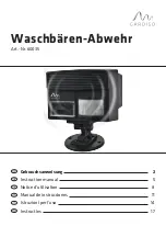
60035
Brand: Gardigo Pages: 19

856
Brand: Febco Pages: 12

NP200
Brand: HANYOUNG NUX Pages: 74

NP100
Brand: HANYOUNG NUX Pages: 36

DF4
Brand: HANYOUNG NUX Pages: 2

HY Series
Brand: HANYOUNG NUX Pages: 4

Nebula
Brand: MADRIX Pages: 91

Nebula
Brand: MADRIX Pages: 36

Nebula
Brand: MADRIX Pages: 40

MP Series
Brand: YASKAWA Pages: 18
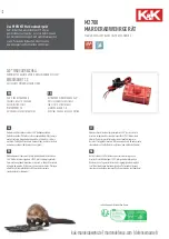
M2700
Brand: K&K Pages: 6

Axiom AIR 25
Brand: M-Audio Pages: 26

Bobbie
Brand: M Climate Pages: 12


