background image

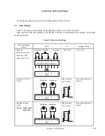
CHAPTER 1  OUTLINE

User’s Manual  U16594EJ1V0UM

15

1.5  Contents in Carton

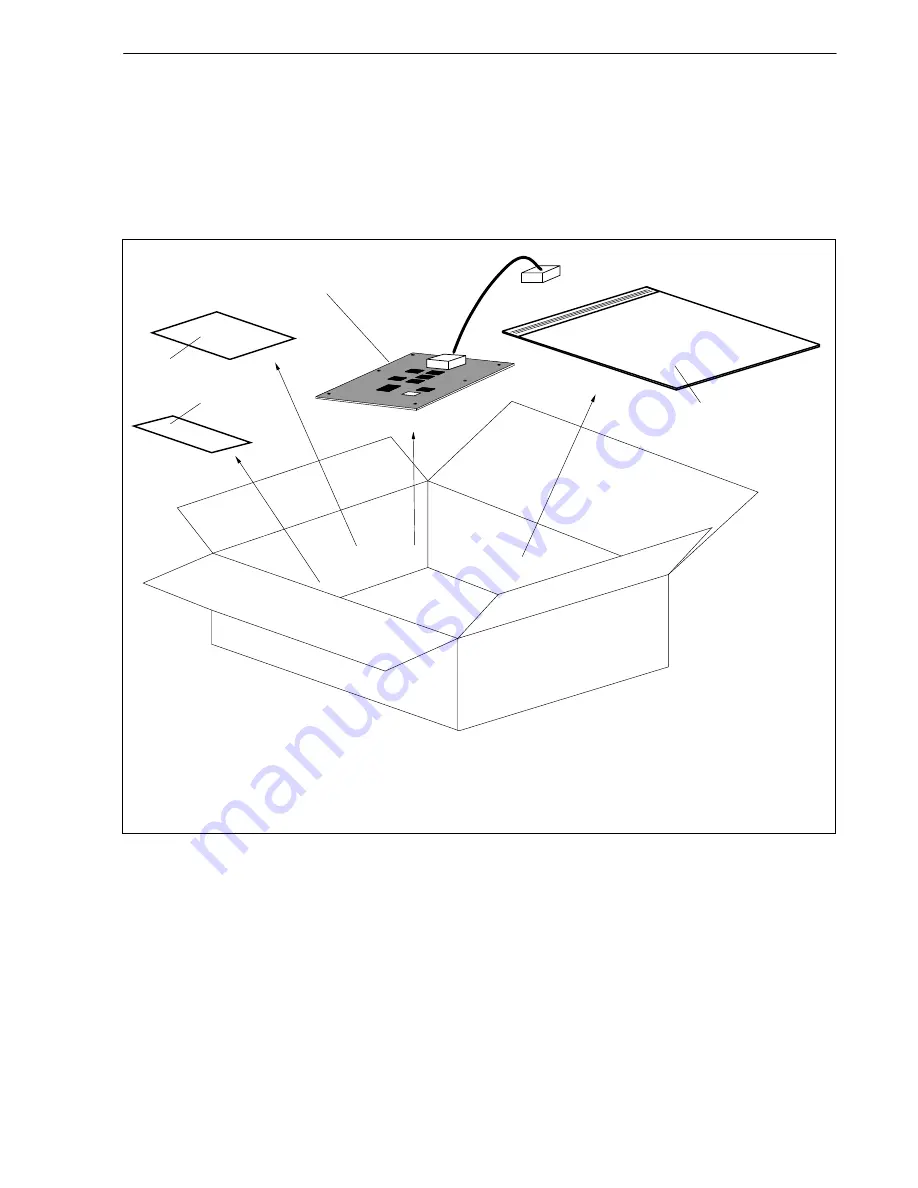
The IE-703217-G1-EM1 package contains the IE-703217-G1-EM1 emulation board, a guarantee card, a packing

list, this manual, and an accessory bag. Check whether the accessory bag contains the items listed below. If you find

any missing or damaged items, contact an NEC Electronics sales representative or distributor.

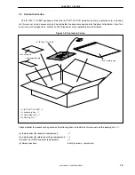
Figure 1-2. Contents in Carton

Check whether the accessory bag contains the following items in addition to this manual and the packing list (

×

 1).

(a) 8-pin header (for resonator replacement):

×

 1

(b) 4-pin header (for reference voltage replacement):

×

 1

(c) Socket (for REGC capacitor replacement):

×

 1

(d) Screws/washers:

6 sets (6 6 washers)

<3> Guarantee card

<4> Packing list

<1> IE-703217-G1-EM1

<2> Accessory bag

<1> IE-703217-G1-EM1 

×

 1 

<2> Accessory bag 

×

 1 

<3> Guarantee card 

×

 1  

<4> Packing list 

×

 1

Summary of Contents for IE-703217-G1-EM1

Page 1: ...User s Manual Target Devices V850ES KF1TM V850ES KG1TM V850ES KJ1TM IE 703217 G1 EM1 Emulation Board Document No U16594EJ1V0UM00 1st edition Date Published September 2003 N CP K Printed in Japan 2003 ...

Page 2: ...User s Manual U16594EJ1V0UM 2 MEMO ...

Page 3: ... enhance the quality reliability and safety of NEC Electronics products customers agree and acknowledge that the possibility of defects thereof cannot be eliminated entirely To minimize risks of damage to property or injury including death to persons arising from defects in NEC Electronics products customers must incorporate sufficient safety measures in their design such as redundancy fire contai...

Page 4: ...nch Seoul Korea Tel 02 558 3737 NEC Electronics Shanghai Ltd Shanghai P R China Tel 021 6841 1138 NEC Electronics Taiwan Ltd Taipei Taiwan Tel 02 2719 2377 NEC Electronics Singapore Pte Ltd Novena Square Singapore Tel 6253 8311 J03 4 NEC Electronics Europe GmbH Duesseldorf Germany Tel 0211 65 03 01 Sucursal en España Madrid Spain Tel 091 504 27 87 Vélizy Villacoublay France Tel 01 30 67 58 00 Succ...

Page 5: ...es functions and configuration parts of the IE V850ES G1 refer to the IE V850ES G1 User s Manual U16313E provided separately To learn about the basic specifications and operation Read this manual in the order listed in CONTENTS To learn software settings such as the operation methods command functions etc of the IE V850ES G1 or IE 703217 G1 EM1 Read the user s manual of the debugger sold separatel...

Page 6: ...U16055E CA850 Ver 2 50 C Compiler Package Assembly Language U16042E ID850 Ver 2 50 Integrated Debugger Operation WindowsTM based U16217E SM850 Ver 2 50 System Simulator Operation Windows based U16218E SM850 Ver 2 00 or Later System Simulator External Part User Open Interface Specifications U14873E Basics U13430E Installation U13410E RX850 Ver 3 13 or Later Real Time OS Technical U13431E Basics U13...

Page 7: ...EM1 16 2 2 LEDs Controlled by IE 703217 G1 EM1 18 CHAPTER 3 SWITCH SETTINGS 19 3 1 Clock Settings 19 3 2 Pull Up Resistor Settings 20 3 3 Power ON Threshold Voltage Settings 21 3 4 Regulator Output Stabilization Capacitance Setting Jumpers 22 CHAPTER 4 SETUP PROCEDURE 23 4 1 Removing Probe and Replacing Clock Module 23 4 2 Removing Emulation Board 25 4 3 Probe Cable Connection 28 CHAPTER 5 CAUTION...

Page 8: ... Closing Cover Step 1 After Removing Front Cover 1 24 4 3 Opening Closing Cover Step 2 Loosening Screws 25 4 4 Opening Closing Cover Step 2 Lifting Front Cover 2 26 4 5 Opening Closing Cover Step 2 After Lifting Front Cover 2 27 4 6 Probe Cable Attachment Position 28 A 1 Equivalent Circuit A 31 A 2 Equivalent Circuit B 31 A 3 Equivalent Circuit C 31 A 4 Equivalent Circuit D 32 A 5 Equivalent Circu...

Page 9: ... Main Clock Settings 19 3 2 Pull Up Resistor Settings 20 3 3 Regulator Output Stabilization Capacitance Settings 22 A 1 Pin Correspondence List V850ES KJ1 Pin Names 35 A 2 Pin Correspondence List V850ES KG1 Pin Names 39 A 3 Pin Correspondence List V850ES KF1 Pin Names 42 ...

Page 10: ...G1 EM1 can be used for efficient hardware and software debugging during system development using the V850ES KF1 V850ES KG1 and V850ES KJ1 This manual describes the basic setup procedure and the switch settings of the IE V850ES G1 when connected to the IE 703217 G1 EM1 For the part names and functions of the IE V850ES G1 refer to the separate IE V850ES G1 User s Manual U16313E ...

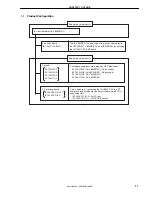
Page 11: ...00 PCI IF A IE 70000 CD IF A This is a board for connecting the IE V850ES G1 to a PC More than one such board can be installed using the PC s expansion slots IE 70000 PCI IF A For PCI bus IE 70000 CD IF A For PCMCIA socket EV 703210GC EV 703210GK EV 703214GC EV 703217GJ Package conversion sockets made by NEC Electronics Separately sold products Sockets EV 703210GC For V850ES KF1 GC package EV 7032...

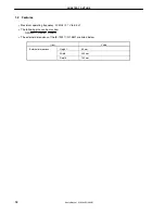
Page 12: ...1 2 Features Maximum operating frequency 20 MHz 2 7 V to 5 5 V The following pins can be masked NMI WAIT RESET HLDRQ The external dimensions of the IE 703217 G1 EM1 are listed below Item Value Height 35 mm Width 205 mm External dimensions Depth 140 mm ...

Page 13: ...External memory 1 MB Internal ROM 256 KB Branch destination entry count calculation coverage memory capacity External memory 1 MB Trace memory capacity 168 bits 32 K frames Time measurement function Internal timers 3 8 bit external trace possible External logic probe Trace break event setting possible Event break Step execution break Forced break Break function Fail safe break Illegal access to pe...

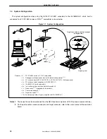
Page 14: ...t connector refer to the user s manual of the emulation board Target system 5 7 4 3 1 2 8 10 9 8 6 9 Target connector connection example enlarged view Target system Remarks 1 PC PC 9800 series or PC AT compatible 2 Debugger sold separately device file obtained separately Note 1 3 PC interface board IE 70000 PCI IF A IE 70000 CD IF A Sold separately 4 PC interface cable supplied with IE V850ES G1 5...

Page 15: ...tact an NEC Electronics sales representative or distributor Figure 1 2 Contents in Carton Check whether the accessory bag contains the following items in addition to this manual and the packing list 1 a 8 pin header for resonator replacement 1 b 4 pin header for reference voltage replacement 1 c Socket for REGC capacitor replacement 1 d Screws washers 6 sets 6 screws 6 washers 3 Guarantee card 4 P...

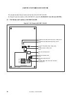
Page 16: ...e 2 1 Part Names of IE 703217 G1 EM1 Emulation probe cable connection connectors CN5 CN6 CN7 X1 OSC2 OSC1 Main clock oscillator socket X1 Regulator output stabilization capacitance setting jumper JP7 1 7 1 8 1 4 JP4 SW1 1 8 JP8 JP7 3 2 1 1 1 CN5 50 50 50 1 1 1 CN7 CN6 GXP AXK KEL IE 703217 G1 EM1 Regulator output stabilization capacitance socket JP8 Power ON threshold voltage setting socket JP4 Pu...

Page 17: ...p resistance which is a mask option of the V850ES KF1 V850ES KG1 and V850ES KJ1 For details refer to 3 2 Pull Up Resistor Settings 6 Power ON threshold voltage setting socket JP4 This socket is used to set the threshold voltage for judging whether the target system is connected For details refer to 3 3 Power ON Threshold Voltage Settings 7 Regulator output stabilization capacitance socket JP8 This...

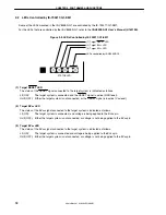
Page 18: ... target system is not connected or the RESET signal is inactive VDD level 2 Target BVDD LED The status of the BVDD signal connected to the target system is indicated as follows Lit ON The target system is connected and voltage is being applied to the BVDD pin Unlit OFF Either the target system is not connected or voltage is not being applied to the BVDD pin 3 Target EVDD LED The status of the EVDD...

Page 19: ...d Table 3 1 Main Clock Settings Main Clock Supply Source OSC1 X1 Debugger Setting Resonator Settings at shipment Resonator 4 MHz Capacitance 15 pF don t care don t care Oscillator on IE 703217 G1 EM1 Mount oscillator on X1 socket 1 2 3 6 7 5 4 8 5V Clock output Set configuration clock to Internal Oscillator on target system Caution Always input a square wave Mount oscillator on X1 socket 1 2 3 6 7...

Page 20: ...or emulation which is a mask option of the V850ES KF1 V850ES KG1 and V850ES KJ1 For the location of SW1 refer to Figure 2 1 Table 3 2 Pull Up Resistor Settings SW1 Port 1 P36 2 P37 3 P38 4 P39 5 P614 6 P615 7 Not used 8 Not used ON Connect pull up resistor OFF Don t connect pull up resistor Remark All the settings are OFF at shipment ...

Page 21: ...his threshold voltage insert a 4 pin jumper standard accessory on which resistors have been mounted to JP4 as shown in Figure 3 2 For the location of JP4 refer to Figure 2 1 Figure 3 1 JP4 Settings at Shipment Figure 3 2 Changing Power ON Threshold Voltage The threshold voltage can be obtained with the following equation Threshold voltage 5 V R2 R1 R2 JP4 3 9 kΩ 1 2 3 4 2 kΩ 5 V Voltage comparator...

Page 22: ...g the regulator of the V850ES KF1 V850ES KG1 or V850ES KJ1 For the location of JP7 and JP8 refer to Figure 2 1 A 10 µF electrolytic capacitor is mounted on JP8 at shipment Table 3 3 Regulator Output Stabilization Capacitance Settings Regulator JP7 JP8 Don t use setting at shipment don t care Use 1 2 JP8 1 2 2 pin jumper standard accessory Output stabilization capacitance To REGC pin of emulation C...

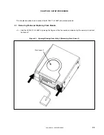
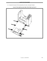
Page 23: ...nect the IE 703217 G1 EM1 and related products 4 1 Removing Probe and Replacing Clock Module 1 Hold the IE 703217 G1 EM1 by placing the fingers at the two locations indicated by the arrows and pull out front cover 1 Figure 4 1 Opening Closing Cover Step 1 Removing Front Cover 1 Front cover 1 ...

Page 24: ...CHAPTER 4 SETUP PROCEDURE User s Manual U16594EJ1V0UM 24 2 Then remove the probe and change the clock Figure 4 2 Opening Closing Cover Step 1 After Removing Front Cover 1 ...

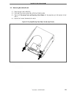
Page 25: ...case down horizontally 2 Disconnect the power supply cable and the host interface cable 3 Refer to 4 1 Removing Probe and Replacing Clock Module for the procedure up to the removal of front cover 1 4 Loosen the 2 screws indicated by the arrows Figure 4 3 Opening Closing Cover Step 2 Loosening Screws ...

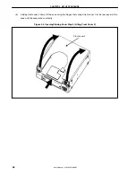
Page 26: ...U16594EJ1V0UM 26 5 Holding front cover 2 down lift the case using the hinges that connect front cover 2 to the rear panel of the case until the case stands vertically Figure 4 4 Opening Closing Cover Step 2 Lifting Front Cover 2 Front cover 2 ...

Page 27: ...APTER 4 SETUP PROCEDURE User s Manual U16594EJ1V0UM 27 6 Remove the 6 screws on the board indicated by the arrows and replace the board Figure 4 5 Opening Closing Cover Step 2 After Lifting Front Cover 2 ...

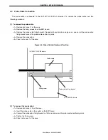
Page 28: ... when doing so as one end of the probe cable fixing bracket covers the probe cable positioning mark 4 Remove the probe cable 5 Close front cover 1 of the case Figure 4 6 Probe Cable Attachment Position 2 To connect the probe cable 1 Remove front cover 1 from the case 2 Insert the probe cable in the socket on the EM1 board 3 Connect the probe cable fixing bracket so that one end covers the probe ca...

Page 29: ... switch of the IE V850ES G1 to OFF V850ES KF1 emulation To perform V850ES KF1 emulation with the target board unconnected do so after connecting the conversion adapter GEA supplied with the EV 703210GK or EV 703210GC to the probe cable If emulation is performed without connecting a conversion adapter the fixed bit values of the following ports become undefined Bits 6 and 7 of port 3 Bits 2 3 4 5 1...

Page 30: ...e operating clock is not initialized to fxx 8 This depends on the timing after reset release 2 Standby mode set release timing The standby mode set release timing differs in the target device and the in circuit emulator When the standby mode is set the timing difference is 1 clock or less and when it is released the difference is 2 to 3 clocks 3 Timing of reset via watchdog timer The reset timing ...

Page 31: ...d in Figures A 1 to A 10 The processing of the target interface for each target device is described in Tables A 1 to A 3 Figure A 1 Equivalent Circuit A Figure A 2 Equivalent Circuit B Figure A 3 Equivalent Circuit C Numbered port other than P9 µPD70F3217 emulation CPU Port pin Target system side IE system side EP1K100FC484 FPGA QS3384Q bus switch Alphabetic port A B HD151015 level shifter A B 5 V...

Page 32: ... a target system is connected Figure A 6 Equivalent Circuit F µPC741G2 operational amplifier VDD EVDD BVDD G6H 2F relayNote µPC393G2 comparator 1 MΩ 100 Ω 0 1 µF IIx Target system side IE system side RESET HSK120 1 MΩ HSK120 74VHCT00 3 6 V applied only when target system not connected Target system side IE system side AVREF0 AVREF1 µPD70F3217 emulation CPU AVREFX G6H 2F relayNote Target system sid...

Page 33: ...ent Circuit G Figure A 8 Equivalent Circuit H Target system side IE system side µPD70F3217 emulation CPU X1 X2 1 2 3 OSC1 1A 1B 2A 2B 1Y 2Y 74HC157 6 7 5 4 8 VCC X1 5V X2 Open 5 4 8 74LCX04 74LCX04 Target system side AVSS VSS EVSS BVSS IE system side µPD70F3217 emulation CPU AVSS VSS EVSS BVSS ...

Page 34: ...lent Circuit J IE system side µPD70F3217 emulation CPU VPP IC JP7 JP8 2 3 1 2 1 REGC Same potential as VDD of target system or 5 V Same potential as VDD of target system or 5 V VPP IC Target system side REGC Open Open IE system side 1 2 3 OSC2 6 7 5 4 1 MΩ Target system side XT1 XT2 Open Open PD70F3217 emulation CPU XT2 XT1 µ ...

Page 35: ...t J 16 XT2 Equivalent circuit J 17 P02 NMI Equivalent circuit A 18 P03 INTP0 Equivalent circuit A 19 P04 INTP1 Equivalent circuit A 20 P05 INTP2 Equivalent circuit A 21 P06 INTP3 Equivalent circuit A 22 P40 SI00 Equivalent circuit A 23 P41 SO00 Equivalent circuit A 24 P42 SCK00 Equivalent circuit A 25 P30 TXD0 Equivalent circuit A 26 P31 RXD0 Equivalent circuit A 27 P32 ASCK0 Equivalent circuit A ...

Page 36: ...0 Equivalent circuit A 56 P613 TI051 TO05 Equivalent circuit A 57 P614 Equivalent circuit A 58 P615 Equivalent circuit A 59 P80 RXD2 SDA1 Equivalent circuit A 60 P81 TXD2 SCL1 Equivalent circuit A 61 P90 A0 TXD1 KR6 Equivalent circuit C 62 P91 A1 RXD1 KR7 Equivalent circuit C 63 P92 A2 TI020 TO02 Equivalent circuit C 64 P93 A3 TI021 Equivalent circuit C 65 P94 A4 TI030 TO03 Equivalent circuit C 66...

Page 37: ... B 95 PCT0 WR0 Equivalent circuit B 96 PCT1 WR1 Equivalent circuit B 97 PCT2 Equivalent circuit B 98 PCT3 Equivalent circuit B 99 PCT4 RD Equivalent circuit B 100 PCT5 Equivalent circuit B 101 PCT6 ASTB Equivalent circuit B 102 PCT7 Equivalent circuit B 103 BVSS Equivalent circuit H 104 BVDD Equivalent circuit D 105 PDL0 AD0 Equivalent circuit B 106 PDL1 AD1 Equivalent circuit B 107 PDL2 AD2 Equiv...

Page 38: ...t B 127 PDH6 A22 Equivalent circuit B 128 PDH7 A23 Equivalent circuit B 129 P715 ANI15 Equivalent circuit A 130 P714 ANI14 Equivalent circuit A 131 P713 ANI13 Equivalent circuit A 132 P712 ANI12 Equivalent circuit A 133 P711 ANI11 Equivalent circuit A 134 P710 ANI10 Equivalent circuit A 135 P79 ANI9 Equivalent circuit A 136 P78 ANI8 Equivalent circuit A 137 P77 ANI7 Equivalent circuit A 138 P76 AN...

Page 39: ...t J 16 XT2 Equivalent circuit J 17 P02 NMI Equivalent circuit A 18 P03 INTP0 Equivalent circuit A 19 P04 INTP1 Equivalent circuit A 20 P05 INTP2 Equivalent circuit A 21 P06 INTP3 Equivalent circuit A 22 P40 SI00 Equivalent circuit A 23 P41 SO00 Equivalent circuit A 24 P42 SCK00 Equivalent circuit A 25 P30 TXD0 Equivalent circuit A 26 P31 RXD0 Equivalent circuit A 27 P32 ASCK0 Equivalent circuit A ...

Page 40: ...circuit C 54 P911 A11 SOA1 Equivalent circuit C 55 P912 A12 SCKA1 Equivalent circuit C 56 P913 A13 INTP4 Equivalent circuit C 57 P914 A14 INTP5 Equivalent circuit C 58 P915 A15 INTP6 Equivalent circuit C 59 PCS0 CS0 Equivalent circuit B 60 PCS1 CS1 Equivalent circuit B 61 PCM0 WAIT Equivalent circuit B 62 PCM1 CLKOUT Equivalent circuit B 63 PCM2 HLDAK Equivalent circuit B 64 PCM3 HLDRQ Equivalent ...

Page 41: ...valent circuit B 85 PDL14 AD14 Equivalent circuit B 86 PDL15 AD15 Equivalent circuit B 87 PDH0 A16 Equivalent circuit B 88 PDH1 A17 Equivalent circuit B 89 PDH2 A18 Equivalent circuit B 90 PDH3 A19 Equivalent circuit B 91 PDH4 A20 Equivalent circuit B 92 PDH5 A21 Equivalent circuit B 93 P77 ANI7 Equivalent circuit A 94 P76 ANI6 Equivalent circuit A 95 P75 ANI5 Equivalent circuit A 96 P74 ANI4 Equi...

Page 42: ...rcuit J 17 P05 INTP2 Equivalent circuit A 18 P06 INTP3 Equivalent circuit A 19 P40 SI00 Equivalent circuit A 20 P41 SO00 Equivalent circuit A 21 P42 SCK00 Equivalent circuit A 22 P30 TXD0 Equivalent circuit A 23 P31 RXD0 Equivalent circuit A 24 P32 ASCK0 Equivalent circuit A 25 P33 TI000 TO00 Equivalent circuit A 26 P34 TI001 Equivalent circuit A 27 P35 TI010 TO01 Equivalent circuit A 28 P38 SDA0 ...

Page 43: ...T1 WR1 Equivalent circuit B 55 PCT4 RD Equivalent circuit B 56 PCT6 ASTB Equivalent circuit B 57 PDL0 AD0 Equivalent circuit B 58 PDL1 AD1 Equivalent circuit B 59 PDL2 AD2 Equivalent circuit B 60 PDL3 AD3 Equivalent circuit B 61 PDL4 AD4 Equivalent circuit B 62 PDL5 AD5 Equivalent circuit B 63 PDL6 AD6 Equivalent circuit B 64 PDL7 AD7 Equivalent circuit B 65 PDL8 AD8 Equivalent circuit B 66 PDL9 A...

Page 44: ...S 1 EV 703210GC for 80GC Unit mm Dimensions with GX Probe connected Dimensions with IC mounted 7 2 12 8 25 3 32 39 7 2 14 4 21 8 24 1 Target connector for 80GC TOP VIEW BOTTOM VIEW C1 5 1 1 2 17 17 7 1 39 40 N 80 14 0 65 CTC APAN 2 15 16 12 35 0 65x19 12 35 ...

Page 45: ...W BOTTOM VIEW IC mounting adapter for 80GC TOP VIEW BOTTOM VIEW 703210GC EA B JAPAN 1 2 1 2 1 2 50 49 49 19 29 7 10 75 10 75 JAPAN CN2 2 1 1 1 1 2 1 40 39 7 1 40 MR1 MR2 MR3 1 6 3 2 1 6 C1 5 1 6 703210GC EA B NEC TET 080SB C2 0 24 1 3 R2 5 24 1 GMA80 14 0 65 JAPAN 1 1 1 1 1 2 20 C1 5 7 1 39 40 ...

Page 46: ...0UM 46 2 EV 703210GK for 80GK Unit mm Dimensions with GX Probe connected Dimensions with IC mounted 7 2 12 8 25 3 32 39 7 2 14 4 21 8 21 0 Target connector for 80GK TOP VIEW BOTTOM VIEW C1 5 1 1 2 15 15 7 1 2 13 14 9 5 0 5x19 9 5 GTC80 12 0 5 AL JAPAN ...

Page 47: ...W BOTTOM VIEW IC mounting adapter for 80GK TOP VIEW BOTTOM VIEW 703210GK EA B JAPAN 1 1 1 1 2 1 2 2 2 2 1 1 1 1 2 50 49 49 19 29 7 10 75 10 75 CN1 H JAPAN CN2 2 1 2 1 40 39 7 1 39 CN1 H 40 MR1 MR2 MR3 1 6 3 2 1 6 C1 5 1 6 NEC TET 080SB C2 0 21 3 R2 5 21 18 C1 5 GMA80 12 0 5 JAPAN 1 1 2 7 1 18 ...

Page 48: ...1V0UM 48 3 EV 703214GC for 100GC Unit mm Dimensions with GX Probe connected Dimensions with IC mounted 7 2 12 8 25 3 32 39 7 2 14 4 21 8 23 Target connector for 100GC TOP VIEW BOTTOM VIEW C1 5 1 1 2 17 17 8 GTC100 14 0 5 JAPAN 2 15 16 12 0 5x24 12 0 ...

Page 49: ... for 100GC TOP VIEW BOTTOM VIEW IC mounting adapter for 100GC TOP VIEW BOTTOM VIEW GEA100 14 0 5 JAPAN CN1 CN1 CN2 2 1 2 1 50 50 49 GEA100 14 0 5 JAPAN CN1 1 2 1 2 1 1 1 1 2 50 49 49 19 29 7 C1 5 10 75 10 75 4 4 NEC 23 4 Ø3 2 100SD TET 23 GMA100 14 0 5 JAPAN 1 1 2 20 C1 5 4 4 ...

Page 50: ... for 144GJ Unit mm Dimensions with GX Probe connected Dimensions with IC mounted 7 2 12 8 25 3 32 7 2 14 4 21 8 29 39 Target connector for 144GJ TOP VIEW BOTTOM VIEW TC 144 20 0 5 JAPAN 21 22 2 17 5 0 5x35 17 5 C1 5 50 TC 144 20 0 5 JAPAN 1 1 1 1 1 2 49 23 23 2 2 7 1 7 1 ...

Page 51: ... VIEW BOTTOM VIEW IC mounting adapter for 144GJ TOP VIEW BOTTOM VIEW EA 144 20 0 5 JAPAN CN1 CN3 CN 2 1 2 1 2 1 50 50 49 49 EA 144 20 0 5 JAPAN CN3 CN1 1 2 1 2 1 2 50 49 49 49 19 29 7 C1 5 10 75 10 75 7 1 7 1 C2 0 3 R2 5 29 144 SD TET 29 50 GMA144 20 0 5 JAPAN 1 1 1 1 1 1 2 7 1 7 1 2 49 23 ...

Page 52: ...APPENDIX B EXTERNAL VIEWS User s Manual U16594EJ1V0UM 52 5 Emulation probe cable Unit mm 12 5 3 GXP CABLE EML MADE IN JAPAN NEC GXP CABLE TARGET JAPAN NEC 32 44 400 39 32 ...

Reviews: