July
2009
Rev
0.06
Page 1 of 31
User Guide: SDALTEVK HSMC SDI ADAPTER BOARD
9-Jul-09 Version
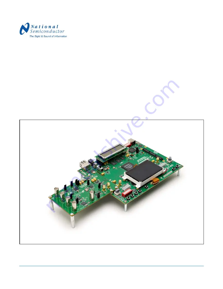
SDI Development Kit using National Semiconductor’s LMH0340 serializer and LMH0341 deserializer
Page 1: ...July 2009 Rev 0 06 Page 1 of 31 User Guide SDALTEVK HSMC SDI ADAPTER BOARD 9 Jul 09 Version 0 06 SDI Development Kit using National Semiconductor s LMH0340 serializer and LMH0341 deserializer ...
Page 2: ...EVALUATION 15 5 2 1 Standalone Mode 16 5 2 2 Pass through Mode 17 5 2 3 Genlocked Mode Error Bookmark not defined 5 3 PUSH BUTTON BASED SD HD 3G SDI EVALUATION 19 5 3 1 Push Button Main Menu 19 5 3 2 System Mode 20 5 3 3 Datapath Menu 20 5 3 4 Video Format Menu 20 5 3 5 Frequency Menu 21 5 4 FPGA REGISTER MAP 21 5 4 1 Miscellaneous Registers 22 5 4 2 Reset Registers 22 5 4 3 Rx Video Registers 22 ...
Page 3: ... Clock Output U5 DS90LV031 A 1 Quad 3V CMOS to LVDS Line Driver Optional Clock Source U2 LP3878 ADJ 1 Micropower 800mA Low Noise Adjustable Voltage Regulator 2 5V Regulator U10 LM20242 1 2A PowerWise Adjustable Frequency Synchronous Buck Regulator 3 3V Regulator U12 Examples of firmware are provided for the Standard Definition SMPTE 259M SD SDI interface the High Definition SMPTE 292M HD SDI inter...
Page 4: ... Rate Standalone mode with multiple format selection o Triple Rate pass thru mode with format detection o Pattern selection o Gen Lock function supported o Register programming supported Altera compiled sof file from ftp ftp altera com outgoing National_SerDes an535_1_0 zip o Triple Rate pass thru mode Quartus II 8 0 or newer http www altera com products Nios II EDS 8 0 http www altera com product...
Page 5: ... bus and LVDS bus signals are supplied to the daughter board through the HSMC connector The Cyclone III FPGA provides the SD HD 3G SDI and general purpose stacks as well as the control interface to a PC through a USB cable This evaluation system allows inexpensive FPGAs to deliver up to 3 Gbps on a coax cable Figure 1 Evaluation Kit Block Diagram Figure 2 Evaluation Kit Connections ...
Page 6: ...one III Development Board 2 2 Cyclone III Development Board Termination Resistors The Altera Cyclone III device does not have any internal termination on the receive LVDS I O s Termination resistors must be added to the Cyclone III board The terminations resistors must be placed as close to the FPGA s pin as possible The 3C120 host board has the layout footprints for the termination resistors Elev...
Page 7: ...July 2009 Rev 0 06 Page 7 of 31 Figure 4 Resistors on HSCM port A Figure 5 Photograph of the back of the Cyclone III board showing location of the 100 Ohm Resistors ...
Page 8: ...receives analog video via BNC connector J2 and provides the HSYNC and VSYNC to the LMH1982 for clock generation The LMH1982 can also generate a clock based on a local 27 MHz oscillator By using the DS90LV031A an external clock can be applied to the card at SMA connector J4 In order to observe the quality of the clock provided to the FPGA the clock can be routed to the DS90LV028A which will drive a...
Page 9: ...ts to download the latest software In order to use the Nios II terminal interface Cygwin must be installed on the PC Visit http www cygwin com to download the latest version of Cygwin for free Make sure that the file cygwin1 dll is installed to the path C altera 80 nios2eds bin Install the Quartus II 8 0 Software Execute the Quartus II 8 0 software installation program The program is called 80_qua...
Page 10: ... and the hardware is powered on and connected to the PC Run Quartus II by either by using the path C altera 80 quartus bin quartus exe or selecting it from the altera folder in the start menu Once the software has loaded go to the Tools menu and select Programmer Figure 7 Quartus Main Screen ...
Page 11: ...Blaster and click Close Use the Add File button to select the appropriate bit image to program the FPGA Make sure that the Program Configure box is checked and that the Mode menu has JTAG selected Press the Start button to program the FPGA Once the progress bar reaches 100 the SDALTEVK is ready to use Figure 8 Quartus Programming Screen ...
Page 12: ...he terminal interface is desired for evaluation run the Nios II terminal program called nios2 terminal exe This program can be found in the bin folder of the Nios II root directory for example C altera 80 nios2eds bin nios2 terminal exe If the software loads correctly a terminal window will appear with a greeting message as shown below Figure 9 Nios II Terminal Main Menu ...
Page 13: ...mission and signal integrity The pattern generator can generate various types of SD HD and 3G SDI static video patterns 4 1 Test Setups 4 1 1 Standalone Video Generator Tests In Standalone mode the system performance can be determined by the internal pattern generator This is done by connecting the serializer output TX1 on J8 to the deserializer input RX on J13 The loop through output of the deser...
Page 14: ...he system is configured to use an analog sync input to generate genlocked video The analog reference signal is applied to the EVK through BNC connector J2 If no analog reference is present the LMH1982 has been configured to automatically switch to the on board oscillator Figure 11 Genlock Test Setup ...
Page 15: ...al Menu Options Menu Option Name Function 1 I2C Read Read from a device register 2 I2C Write Write to a device register 3 Register Read Read from an FPGA register 4 Register Write Write to an FPGA register 5 I2C Bus Scan Returns 7 bit address of all devices on the serial control bus 6 Put System in Standalone Mode Configures system for Standalone Mode Accesses format select menu 7 Put System in An...
Page 16: ...irectly to the left of the format title Once a format is selected the terminal will return to the main menu and the SDALTEVK will then be operating sending a test pattern in the specified SDI video format Once the two digit code is selected the Selected format will be displayed followed by the Main Menu After the main menu a reminder of what mode the system is currently in will be shown Figure 13 ...
Page 17: ...ock Mode In Analog Sync Reclock Mode you provide both an analog Sync input as in the Analog Sync TPG mode and an SDI input which is genlocked to the Analog Sync input The timing information is extracted from the analog signal and a new serial clock is generated using the LMH1982 and this clock is used to reclock the data received through the SDI input port 4 2 4 Analog Sync alternate TPG Mode In A...
Page 18: ...om the main menu apply an SD HD or 3G SDI video signal from an external source to the SDALTEVK When Pass through Mode is selected from the main menu a message will appear notifying if an input signal of a supported format is detected and return to the main menu Figure 15 Pass through Mode Screen ...
Page 19: ...ice and FPGA register access Figure 16 LED and Push Button Locations 4 3 1 Push Button Main Menu After the FPGA has been programmed the push buttons default to the main menu options While in the main menu LED 1 will blink LED 6 7 or 8 will illuminate to indicate the current configuration of the EVK PB 0 PB 1 PB 2 PB 3 System Mode DP Settings Video Format Video Frequency LED 1 LED 2 LED 3 LED 4 LED...
Page 20: ...atch between frequency and video format Genlock No reference or invalid reference Passthrough Input video not present or unrecognized 4 3 3 Datapath Menu This menu will be available in a future release If this menu is selected the LEDs will flash twice and the system will return to the main menu 4 3 4 Video Format Menu The Video Format Menu configures the push buttons to navigate through the suppo...
Page 21: ...01 74 25 MHz HD 010 148 35 MHz 3G 011 148 5 MHz 3G 100 0 0000 525 I PAL 1 0001 486 I NTSC 2 0010 720 P 720P50 3 0011 720 P 720P59 94 720P60 4 0100 1080 S 1080S23 9 8 1080S24 5 0101 1080 I 1080I50 6 0110 1080 I 1080I59 94 1080I60 7 0111 1080 P 1080P23 9 8 1080P24 8 1000 1080 P 1080P25 9 1001 1080 P 1080P29 9 7 1080P30 A 1010 1080 P 1080P50 B 1011 1080 P 1080P59 94 1080P60 Figure 23 Video Format and...
Page 22: ...Rx Video Registers Hex Address Name Description Bits Bit Description 03 RX VID STATUS Status bits of Rx video 15 4 3 2 1 0 Reserved Vid Reset Flag Indicates that video reset has been asserted Deser Flag Indicates that the deserializer lock has toggled Descram Flag Indicates that the descrambler lock has toggled Descram Locked Indicates that the descrambler is locked onto incoming video 04 RX VID S...
Page 23: ...C Error Count 06 CRC CONTROL CRC Check Control 15 3 2 1 0 Reserved Select Holdover Mode Reset Status flags Reset CRC Error Count 07 EDH STATUS 1 EDH Error Check Status Reg 15 14 10 9 5 4 0 Reserved Full Field error flags Active Picture error flags ANC flags 08 EDH STATUS 2 EDH Error Check Status Reg 2 15 14 12 11 8 7 4 3 2 1 0 EDH Present EDH Detection Count indicates intermittent EDH Full Frame C...
Page 24: ...E35212 Extracted SMPTE352 Bytes 1 2 15 0 SMPTE352 Bytes 2 and 1 0E AUDIO IN CONTROL I2S Output Control 15 1 0 Reserved Enable I2S Output 5 1 4 Datapath Registers Hex Address Name Description Bits Bit Description 10 DP STATUS Datapath Status Register 15 0 Reserved 11 DP CONTROL 15 14 7 6 5 4 3 2 1 0 Data Pat Bypass Reserved Insert CRC EDH Errors on output Insert EDH Packets on output Insert SMPTE35...
Page 25: ...nel 2 Frequency 17 AUDIO OUT INCR 2 Controls Increment Rate for Internal Tone Generator 15 8 7 0 Channel 3 Frequency Channel 4 Frequency 18 AUDIO OUT CSB 1 Controls Audio CSB 15 8 7 0 Channel Status Block CRC Channel Status Block Byte 2 19 AUDIO OUT CSB 2 Controls Audio CSB 15 8 7 0 Channel Status Block Byte 1 Channel Status Block Byte 0 1A TEST PATTERN CONTROL Select Output test Pattern 15 14 13 ...
Page 26: ... Enable Reserved Update adress 5 1 5 Clocking Hex Address Name Description Bits Bit Description 20 CLOCK STATUS ALTERA Status of ALtera PLLs 15 3 2 1 0 Reserved Active clock specified whether the receive 0 or PLL 1 clock is for transmission Tx PLL Locked Rx PLL Locked 21 CLOCK CONTROL ALTERA Control Altera Clock selection 15 14 0 Select PLL 1 or Rx 0 Clock Reserved 5 1 6 Video Timing Hex Address N...
Page 27: ...10 0 Reserved Decoded format type 000 0 Unknown 001 1 PAL 010 2 NTSC 011 3 576P 100 4 480P 101 5 720P 110 6 1080I 111 7 1080P Reserved Vformat received from LMH1981 26 LINE TIME COUNT Used to Determine Format See Genlock_if module for details 15 0 Line time count 16 MSB 27 STATUS GENFORMAT Format Used to Drive Timing Generator 15 11 10 8 7 4 3 0 Reserved Frequency selected as per RX VID FREQ Reser...
Page 28: ...July 2009 Rev 0 06 Page 28 of 31 Hex Address Name Description Bits Bit Description 7 0 Counts when timing is resynchronized ...
Page 29: ...est Patterns The following test patterns are available from the SDI firmware in all SD HD and 3G formats 100 Color Bars Frequency Sweep Black Matrix Pathological Luma Ramp Y C Full Range Ramp SMPTE 75 Color Bars SMPTE RP219 Color Bars Luma Pulse Bar ...
Page 30: ...he SDALTEVK can be found on the EVK website 8 Reference FPGA IP The reference FPGA IP source code and documentation can be found on EVK website 9 Up to Date Information For up to date information check this URL http www national com sdaltevk 10 Part Numbers Cyclone III Development Board DK DEV 3C120N http www altera com products devkits altera kit cyc3 html LMH0340 LMH0341 Evaluation Kit SDALTEVK ...
Page 31: ...s Column widths 0 03 8 28 2008 N Unger Put revision history at the end Change font of the TOC to Ariel Inserted termination resistor instructions Minor wording changes on Table 1 0 04 9 02 2008 N Unger Updated Altera Part Number to DK DEV 3C120N 0 05 9 03 2008 N Unger Recovered File Changed date format in the revision history 0 06 07 09 2009 M Sauerwald Updated for December 2008 IP release ...
Page 32: ...for use in safety critical applications such as life support where a failure of the TI product would reasonably be expected to cause severe personal injury or death unless officers of the parties have executed an agreement specifically governing such use Buyers represent that they have all necessary expertise in the safety and regulatory ramifications of their applications and acknowledge and agre...