background image

Chapter 2

Hardware Overview of the NI 7831R

NI 7831R User Manual

2-20

ni.com

the remaining devices on that PXI bus segment must have PXI/TRIG0 
configured as an input.

Caution

Do 

not 

drive the same RTSI trigger bus line with the NI 7831R and another device 

simultaneously. Such signal driving can damage both devices. NI is 

not

 liable for any 

damage resulting from such signal driving.

For more information on using and configuring triggers, select 

Help»VI, 

Function, & How-To Help

 in LabVIEW to view the 

LabVIEW Help

Refer to the 

PXI Hardware Specification Revision 2.1

 and 

PXI Software 

Specification Revision 2.1

 at 

pxisa.org

 for more information about PXI 

triggers.

PXI Local Bus (for NI PXI-7831R only)

The NI PXI-7831R can communicate with other PXI devices using the PXI 
local bus. The PXI local bus is a daisy-chained bus that connects each PXI 
peripheral slot with its adjacent peripheral slot on either side. For example, 
the right local bus lines from a PXI peripheral slot connect to the left local 
bus lines of the adjacent slot on the right. Each local bus is 13 lines wide. 
All of these lines connect to the FPGA on the NI PXI-7831R. The PXI local 
bus right lines on the NI PXI-7831R are PXI/LBR<0..12>. The PXI local 
bus left lines on the NI PXI-7831R are PXI/LBLSTAR<0..12>.

The NI PXI-7831R can configure each PXI local bus line either as an input 
or an output signal. Only one device can drive the same physical local bus 
line at a time. For example, if the NI PXI-7831R is configured to drive a 
signal on PXI/LBR 0, the device in the slot immediately to the right must 
have its PXI/LBLSTAR 0 line configured as an input.

Caution

Do 

not 

drive the same PXI local bus line with the NI PXI-7831R and another 

device simultaneously. Such signal driving can damage both devices. NI is 

not 

liable for 

any damage resulting from such signal driving.

The NI PXI-7831R local bus lines are only compatible with 3.3 V signaling 
LVTTL and LVCMOS levels.

Caution

Do 

not

 enable the local bus lines on an adjacent device if the device drives 

anything other than 0–3.3V LVTTL signal levels on the NI PXI-7831R. Enabling the lines 
in this way can damage the NI PXI-7831R. NI is 

not 

liable for any damage resulting from 

enabling such lines.

Summary of Contents for NI 7831R

Page 1: ...Reconfigurable I O NI 7831R User Manual Reconfigurable I O Devices for PCI PXI CompactPCI Bus Computers NI 7831R User Manual April 2004 Edition Part Number 370489B 01 ...

Page 2: ...9 741 31 30 Greece 30 2 10 42 96 427 India 91 80 51190000 Israel 972 0 3 6393737 Italy 39 02 413091 Japan 81 3 5472 2970 Korea 82 02 3451 3400 Malaysia 603 9131 0918 Mexico 001 800 010 0793 Netherlands 31 0 348 433 466 New Zealand 0800 553 322 Norway 47 0 66 90 76 60 Poland 48 22 3390150 Portugal 351 210 311 210 Russia 7 095 783 68 51 Singapore 65 6226 5886 Slovenia 386 3 425 4200 South Africa 27 ...

Page 3: ...ration or maintenance instructions owner s modification of the product owner s abuse misuse or negligent acts and power failure or surges fire flood accident actions of third parties or other events outside reasonable control Copyright Under the copyright laws this publication may not be reproduced or transmitted in any form electronic or mechanical including photocopying recording storing in an i...

Page 4: ...ent of Communications DOC Changes or modifications not expressly approved by NI could void the user s authority to operate the equipment under the FCC Rules Class A Federal Communications Commission This equipment has been tested and found to comply with the limits for a Class A digital device pursuant to part 15 of the FCC Rules These limits are designed to provide reasonable protection against h...

Page 5: ...re 1 4 Reconfigurable I O Applications 1 5 Software Development 1 5 LabVIEW FPGA Module 1 5 LabVIEW Real Time Module 1 6 Cables and Optional Equipment 1 7 Custom Cabling 1 8 Safety Information 1 9 Chapter 2 Hardware Overview of the NI 7831R Analog Input 2 3 Input Modes 2 4 Input Range 2 4 Connecting Analog Input Signals 2 5 Types of Signal Sources 2 7 Floating Signal Sources 2 7 Ground Referenced ...

Page 6: ...ting Analog Output Signals 2 15 Digital I O 2 16 Connecting Digital I O Signals 2 16 RTSI Trigger Bus 2 19 PXI Local Bus for NI PXI 7831R only 2 20 Switch Settings 2 21 Power Connections 2 22 Field Wiring Considerations 2 23 Chapter 3 Calibration Loading Calibration Constants 3 1 Internal Calibration 3 1 External Calibration 3 2 Appendix A Specifications Appendix B Connecting I O Signals Appendix ...

Page 7: ... down the File menu select the Page Setup item and select Options from the last dialog box This icon denotes a note which alerts you to important information This icon denotes a caution which advises you of precautions to take to avoid injury data loss or a system crash When this symbol is marked on the device refer to the Safety Information section of Chapter 1 Introduction for precautions to tak...

Page 8: ...lect Start Program Files National Instruments LabVIEW Module Documents LabVIEW FPGA Release Notes to view this document LabVIEW FPGA Module User Manual This manual describes how to use the LabVIEW FPGA Module to create virtual instruments VIs that run on the NI 7831R Select Start Program Files National Instruments LabVIEW Module Documents FPGA User Interface to view this document FPGA Interface Us...

Page 9: ...Documentation The following documents contain information you might find helpful NI Developer Zone tutorial Field Wiring and Noise Considerations for Analog Signals at ni com zone PICMG CompactPCI 2 0 R3 0 PXI Hardware Specification Revision 2 1 PXI Software Specification Revision 2 1 ...

Page 10: ...custom virtual instrument VI to the FPGA Using the FPGA Module you can graphically design the timing and functionality of the R Series device If you only have LabVIEW but not the FPGA Module you cannot create new FPGA VIs but you can create VIs that run on Windows or an RT target to control existing FPGA VIs Some applications require tasks such as real time floating point processing or datalogging...

Page 11: ...pactPCI specification permits vendors to develop sub buses that coexist with the basic PCI interface on the CompactPCI bus Compatible operation is not guaranteed between CompactPCI devices with different sub buses nor between CompactPCI devices with sub buses and PXI The standard implementation for CompactPCI does not include these sub buses The R Series device works in any standard CompactPCI cha...

Page 12: ...plication requirements and to mimic the functionality of fixed I O devices For example you can configure a R Series device in one application for three 32 bit quadrature encoders and then reconfigure the R Series device in another application for eight 16 bit event counters You also can use the R Series device in timing and triggering applications with the LabVIEW Real Time Module such as control ...

Page 13: ...mathematical operations You can implement multiple functions efficiently in the same design operating sequentially or in parallel You can implement more complex algorithms such as control loops You are limited only by the size of the FPGA Reconfigurable I O Architecture Figure 1 1 shows an FPGA connected to fixed I O resources and a bus interface The fixed I O resources include A D converters ADCs...

Page 14: ...iting for the computer to completely boot and load the FPGA Refer to the LabVIEW FPGA Module User Manual for more information about how to store your VI in flash memory Reconfigurable I O Applications You can use the LabVIEW FPGA Module to create or acquire new VIs for your application The FPGA Module allows you to define custom functionality for the R Series device using a subset of LabVIEW funct...

Page 15: ... can use the utility to configure the analog input mode to synchronize the clock R Series device to the PXI clock for NI PXI 7831R only and to configure when the VI loads from flash memory LabVIEW Real Time Module The LabVIEW Real Time Module extends the LabVIEW development environment to deliver deterministic real time performance You can write host VIs that run in Windows or on RT targets to com...

Page 16: ...0 050 series D type connector The cable is constructed with 34 twisted wire pairs and an overall shield MIO or DIO Connects to the following standard 68 pin screw terminal blocks SCB 68 CB 68LP CB 68LPR TBX 68 SMC68 68 RMIO Shielded 68 pin VHDCI male connector to female 0 050 series D type connector The cable is constructed with individually shielded twisted pairs for the analog input channels plu...

Page 17: ...s NSC68 262650 Non shielded cable connects from 68 pin VHDCI male connector to two 26 pin female headers plus one 50 pin female header The pinout of these headers allows for direct connection to 5B backplanes for analog signal conditioning and SSR backplanes for digital signal conditioning MIO only 26 pin headers can connect to the following 5B backplanes for analog signal conditioning 5B08 8 chan...

Page 18: ...e If you need to clean the NI 7831R use a soft nonmetallic brush Make sure that the NI 7831R is completely dry and free from contaminants before returning it to service Operate the NI 7831R only at or below Pollution Degree 2 Pollution is foreign matter in a solid liquid or gaseous state that can reduce dielectric strength or surface resistivity The following is a description of pollution degrees ...

Page 19: ...cal distribution such as that provided by a standard wall outlet for example 115 V for U S or 230 V for Europe Examples of Installation Category II are measurements performed on household appliances portable tools and similar products Installation Category III Measurements performed in the building installation at the distribution level This category refers to measurements on hard wired equipment ...

Page 20: ...7831R Figure 2 1 NI 7831R Block Diagram AI AI PCI PXI CompactPCI Bus Input Mux Instrumentation Amplifier Input Mode Mux AISENSE AIGND 16 Bit DAC x8 Channels 2 x8 Channels Configuration Flash Memory User Configurable FPGA on RIO Devices Bus Interface Connector 1 DIO Connector 2 DIO Data Address Control Digital I O 16 Digital I O 40 Digital I O 40 Calibration DACs Configuration Control Connector 0 M...

Page 21: ...Chapter 2 Hardware Overview of the NI 7831R NI 7831R User Manual 2 2 ni com Figure 2 2 Parts Locator Diagram for the NI PXI 7831R SW1 ...

Page 22: ...e NI PCI 7831R Analog Input The NI 7831R has eight independent 16 bit AI channels that you can sample simultaneously or at different rates The input mode is software configurable and the input range is fixed at 10 V The converters return data in two s complement format Table 2 1 shows the ideal output code returned for a given AI voltage SW1 ...

Page 23: ...2 2 Available Input Modes for the NI 7831R Input Mode Description DIFF When the NI 7831R is configured in DIFF input mode each channel uses two AI lines The positive input pin connects to the positive terminal of the onboard instrumentation amplifier The negative input pin connects to the negative input of the instrumentation amplifier RSE When the NI 7831R is configured in RSE input mode each cha...

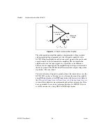
Page 24: ...o AIGND In NRSE input mode the AISENSE signal is connected internally to the negative input of the instrumentation amplifier for each channel In DIFF and RSE input modes AISENSE is not used Caution Exceeding the differential and common mode input ranges distorts the input signals Exceeding the maximum input voltage rating can damage the NI 7831R and the computer NI is not liable for any damage res...

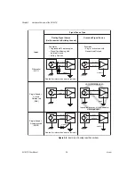
Page 25: ... The amplifier output voltage is referenced to the device ground The NI 7831R ADC measures this output voltage when it performs A D conversions You must reference all signals to ground either at the source device or at the NI 7831R If you have a floating source reference the signal to ground by using RSE input mode or the DIFF input mode with bias resistors Refer to the Differential Connections fo...

Page 26: ...ts out of the common mode input range Ground Referenced Signal Sources A ground referenced signal source is connected to the building system ground so it is already connected to a common ground point with respect to the NI 7831R assuming that the computer is plugged into the same power system Instruments or devices with nonisolated outputs that plug into the building power system are ground refere...

Page 27: ...g are added to measured signal NOT RECOMMENDED V1 AI i AI i AIGND i V1 AI i AI i AIGND i See text for information on bias resistors Signal Source Type Floating Signal Source Not Connected to Building Ground Grounded Signal Source Examples Ungrounded Thermocouples Signal Conditioning with Isolated Outputs Battery Devices Examples Plug in Instruments with Nonisolated Outputs Input Differential DIFF ...

Page 28: ...se differential input connections for any channel that meets any of the following conditions The input signal is low level less than 1 V The leads connecting the signal to the NI 7831R are greater than 3 m 10 ft The input signal requires a separate ground reference point or return signal The signal leads travel through noisy environments Differential signal connections reduce noise pickup and incr...

Page 29: ... the leads connecting the signal sources to the device The instrumentation amplifier can reject common mode signals when V in and V in input signals are both within their specified input ranges Refer to Appendix A Specifications for more information about input ranges Differential Connections for Nonreferenced or Floating Signal Sources Figure 2 7 shows how to connect a floating signal source to a...

Page 30: ...arger source impedances this connection leaves the differential signal path significantly out of balance Noise that couples electrostatically onto the positive line does not couple onto the negative line because it is connected to ground Hence this noise appears as a differential mode signal instead of a common mode signal and the instrumentation amplifier does not reject it In this case instead o...

Page 31: ...as high output impedance balance the signal path as previously described using the same value resistor on both the positive and negative inputs Loading down the source causes some gain error Single Ended Connection Considerations When the NI 7831R AI signal is referenced to a ground that can be shared with other input signals it forms a single ended connection The input signal connects to the posi...

Page 32: ...e NI 7831R configured for RSE input mode Figure 2 8 Single Ended Input Connections for Nonreferenced or Floating Signals Single Ended Connections for Grounded Signal Sources NRSE Input Mode To measure a grounded signal source with a single ended input mode you must configure the NI 7831R in the NRSE input mode Then connect the signal to the positive input of the NI 7831R instrumentation amplifier ...

Page 33: ...tions for signal sources that are already referenced to some ground point with respect to the NI 7831R In these cases the instrumentation amplifier can reject any voltage caused by ground potential differences between the signal source and the device With differential input connections the instrumentation amplifier can reject common mode noise pickup in the leads connecting the signal sources to t...

Page 34: ... ideal AO voltage generated for a given input code Note If your VI does not set the output value for an AO channel then the AO channel voltage output will be undefined Connecting Analog Output Signals The AO signals are AO 0 7 and AOGND AO 0 7 are the eight available AO channels AOGND is the ground reference signal for the AO channels Figure 2 10 shows how to make AO connections to the NI 7831R Ta...

Page 35: ...DIO 0 39 The DIO 0 n signals make up the DIO port and DGND is the ground reference signal for the DIO port The NI 7831R has one MIO and two DIO connectors for a total of 96 DIO lines Refer to Figure B 1 NI 7831R Connector Locations and Figure B 2 NI 7831R I O Connector Pin Assignments for the connector locations and the I O connector pin assignments on the NI 7831R The DIO lines on the NI 7831R ar...

Page 36: ...any damage resulting from such signal connections Caution Do not short the DIO lines of the NI 7831R directly to power or to ground Doing so can damage the NI 7831R by causing excessive current to flow through the DIO lines You can connect multiple NI 7831R digital output lines in parallel to provide higher current sourcing or sinking capability If you connect multiple digital output lines in para...

Page 37: ...lications include sending TTL or LVCMOS signals and driving external devices such as the LED shown in Figure 2 11 The NI 7831R SH68 C68 S shielded cable contains 34 twisted pairs of conductors To maximize the digital I O available on the NI 7831R some of the DIO lines are twisted with power or ground and some DIO lines are twisted with other DIO lines To obtain maximum signal integrity place edge ...

Page 38: ...o any other device that supports RTSI triggers On the NI PCI 7831R the RTSI trigger lines are labeled RTSI TRIG 0 6 and RTSI OSC On the NI PXI 7831R the RTSI trigger lines are labeled PXI TRIG 0 7 In addition the NI PXI 7831R can use the PXI star trigger line to send or receive triggers from a device plugged into Slot 2 of the PXI chassis The PXI star trigger line on the NI PXI 7831R is PXI STAR T...

Page 39: ...nes of the adjacent slot on the right Each local bus is 13 lines wide All of these lines connect to the FPGA on the NI PXI 7831R The PXI local bus right lines on the NI PXI 7831R are PXI LBR 0 12 The PXI local bus left lines on the NI PXI 7831R are PXI LBLSTAR 0 12 The NI PXI 7831R can configure each PXI local bus line either as an input or an output signal Only one device can drive the same physi...

Page 40: ...ing can damage the NI 7831R and the other device NI is not liable for any damage resulting from such signal driving Refer to the PXI Hardware Specification Revision 2 1 and PXI Software Specification Revision 2 1 at www pxisa org for more information about PXI triggers Switch Settings Refer to Figure 2 2 for the location of switch SW1 on the NI PXI 7831R and Figure 2 3 for the location of switch S...

Page 41: ...n the NI 7831R is powered on with switch 1 in the ON position the analog circuitry does not return properly calibrated data Move the switch to the ON position only while you are using software to reconfigure the NI 7831R for the desired power up behavior Afterward return switch 1 to the OFF position Power Connections Two pins on each I O connector supply 5 V from the computer power supply using a ...

Page 42: ...d for signals traveling through areas with large magnetic fields or high electromagnetic interference Route signals to the device carefully Keep cabling away from noise sources The most common noise source in a PXI DAQ system is the video monitor Keep the monitor and the analog signals as far apart as possible Use the following recommendations for all signal connections to the NI 7831R Separate NI...

Page 43: ...the levels indicated in Appendix A Specifications The onboard nonvolatile flash memory stores the calibration constants for the device Calibration constants are the values that were written to the CalDACs to achieve calibration in the factory The NI 7831R hardware reads these constants from the flash memory and loads them into the CalDACs at power on This occurs before you load a VI into the FPGA ...

Page 44: ... reference rather than relying on the onboard reference The NI 7831R has an onboard calibration reference to ensure the accuracy of self calibration The reference voltage is measured at the factory and stored in the flash memory for subsequent internal calibrations Externally calibrate the device annually or more often if you use it at extreme temperatures During the external calibration process t...

Page 45: ...RSE NRSE software selectable selection applies to all 8 channels Type of ADC Successive approximation Resolution 16 bits 1 in 65 536 Conversion time 4 µs Maximum sampling rate 200 kS s per channel Input impedance Powered on 10 GΩ in parallel with 100 pF Powered off 4 kΩ min Overload 4 kΩ min Input signal range 10 V Input bias current 2 nA Input offset current 1 nA Input coupling DC Maximum working...

Page 46: ... Range V Absolute Accuracy Relative Accuracy of Reading Offset µV Noise Quantization µV Temp Drift C Absolute Accuracy at Full Scale mV Resolution µV Positive Full Scale Negative Full Scale 24 Hours 1 Year Single Point Averaged Single Point Averaged 10 0 10 0 0 0496 0 0507 2542 1779 165 0 0005 7 78 2170 217 Note Accuracies are valid for measurements following an internal calibration Measurement ac...

Page 47: ...20 0 V 7 5 µs 10 3 µs 40 µs 2 0 V 2 7 µs 4 1 µs 5 1 µs 0 2 V 1 7 µs 2 9 µs 3 6 µs Nominal Range V Absolute Accuracy Absolute Accuracy at Full Scale mV of Reading Offset µV Temp Drift C Positive Full Scale Negative Full Scale 24 Hours 1 Year 10 0 10 0 0 0335 0 0351 2366 0 0005 5 88 Note Accuracies are valid for analog output following an internal calibration Analog output accuracies are listed for ...

Page 48: ...mpedance 1 25 Ω Current drive 2 5 mA Protection Short circuit to ground Power on state User configurable Dynamic Characteristics Settling time Slew rate 10 V µs Noise 150 µVrms DC to 1 MHz Glitch energy at midscale transition 200 mV for 3 µs Digital I O Number of channels 96 input output Compatibility TTL Step Size Accuracy 16 LSB 4 LSB 2 LSB 20 0 V 6 0 µs 6 2 µs 7 2 µs 2 0 V 2 2 µs 2 9 µs 3 8 µs ...

Page 49: ...ay be shorted at a time Reconfigurable FPGA Number of logic slices 5 120 Equivalent number of logic cells 11 520 Available embedded RAM 81 920 bytes Timebase 40 80 120 160 or 200 MHz Timebase reference sources NI PCI 7831R Onboard clock only NI PXI 7831R Onboard clock phase locked to PXI 10 MHz clock Timebase accuracy Onboard clock 100 ppm 250 ps jitter Level Min Max Input low voltage VIL Input hi...

Page 50: ... 000 V 3 5 mV actual value stored in Flash memory Temperature coefficient 5 ppm C max Long term stability 20 ppm Note Refer to Calibration Certificates at ni com calibration to generate a calibration certificate for the NI 7831R Bus Interface PXI NI PXI 7831R only Master slave PCI NI PCI 7831R only Master slave Power Requirement 5 VDC 5 450 mA typ 700 mA max does not include current drawn from the...

Page 51: ...6 7 in by 4 3 in I O connectors Three 68 pin female high density VHDCI type Maximum Working Voltage Maximum working voltage refers to the signal voltage plus the common mode voltage Channel to earth 12 V Installation Category I Channel to channel 24 V Installation Category I Environmental The NI 7831R is intended for indoor use only Operating Environment Using 40 MHz timebase 0 to 55 C tested in a...

Page 52: ...95 noncondensing tested in accordance with IEC 60068 2 56 Note Clean the device with a soft non metallic brush Make sure that the device is completely dry and free from contaminants before returning it to service Shock and Vibration for NI PXI 7831R Only Operational Shock 30 g peak half sine 11 ms pulse Tested in accordance with IEC 60068 2 27 Test profile developed in accordance with MIL PRF 2880...

Page 53: ...patibility Emissions EN 55011 Class A at 10 m FCC Part 15A above 1 GHz Immunity EN 61326 1997 A2 2001 Table 1 EMC EMI CE C Tick and FCC Part 15 Class A compliant Note For full EMC compliance operate this device with shielded cabling CE Compliance This product meets the essential requirements of applicable European Directives as amended for CE marking as follows Low Voltage Directive safety 73 23 E...

Page 54: ...NI 7831R has two DIO connectors with 40 DIO lines per connector and one MIO connector with eight AI lines eight AO lines and 16 DIO lines Figure B 1 shows the I O connector locations for the NI PXI 7831R and the NI PCI 7831R Figure B 1 NI 7831R Connector Locations NI PXI 7831R CONNECTOR 0 MIO CONNECTOR 1 DIO CONNECTOR 2 DIO Reconfigurable I O CONNECTOR 0 MIO CONNECTOR 1 DIO CONNECTOR 2 DIO ...

Page 55: ...DGND DGND DGND 5V 5V DIO28 DIO30 DIO32 DIO34 DIO36 DIO38 DIO0 DIO2 DIO3 DIO5 DIO6 DIO7 DIO8 DIO1 DIO4 DIO9 DIO10 DIO11 DIO12 DIO13 DIO14 DIO15 DIO16 DIO17 DIO18 DIO19 DIO20 DIO21 DIO22 DIO23 DIO24 DIO25 DIO26 DIO27 DIO29 DIO31 DIO33 DIO35 DIO37 DIO39 1 35 2 36 3 37 4 38 5 39 6 40 7 41 8 42 9 43 10 44 11 45 12 46 13 47 14 48 15 49 16 50 17 51 18 52 19 53 20 54 21 55 22 56 23 57 24 58 25 59 26 60 27...

Page 56: ...hrough 7 AIGND Analog Input Ground These pins are the reference point for single ended measurements in RSE configuration and the bias current return point for differential measurements All three ground references AIGND AOGND and DGND are connected to each other on the NI 7831R AISENSE AIGND Input Analog Input Sense This pin serves as the reference node for AI 0 7 when the device is configured for ...

Page 57: ...31R I O Signal Summary Signal Name Signal Type and Direction Impedance Input Output Protection Volts On Off Source mA at V Sink mA at V Rise Time Bias 5V DO AI 0 7 AI 10 GΩ in parallelwith 100 pF 42 35 2 nA AI 0 7 AI 10 GΩ in parallelwith 100 pF 42 35 2 nA AIGND AO AISENSE AI 10 GΩ in parallelwith 100 pF 42 35 2 nA AO 0 7 AO 1 25 Ω Short circuit to ground 2 5 at 10 2 5 at 10 10 V µs AOGND AO DGND ...

Page 58: ...nal conditioning The other 26 pin header contains all the NI 7831R analog output signals You can plug this connector directly into a 5B backplane for AO signal conditioning The NI 7831R AO 0 7 correspond to the 5B backplane channels 0 7 in sequential order The 50 pin header contains the 16 DIO lines available on the NI 7831R MIO connector You can plug this header directly into an SSR backplane for...

Page 59: ...pond to Slots 0 15 on an SSR backplane in sequential order You can connect to an SSR backplane containing a number of channels unequal to the number of lines on the 2 4 6 8 10 12 14 16 18 20 22 24 26 1 3 5 7 9 11 13 15 17 19 21 23 25 AO0 AOGND0 AO1 AO2 AOGND2 AO3 AO4 AOGND4 AO5 AO6 AOGND6 AO7 NC NC NC AOGND1 NC NC AOGND3 NC NC AOGND5 NC NC AOGND7 NC AO 0 7 Connector Pin Assignment 2 4 6 8 10 12 14...

Page 60: ...3 35 37 39 41 43 45 47 49 DIO23 DIO22 DIO21 DIO20 DIO19 DIO18 DIO17 DIO16 DIO15 DIO14 DIO13 DIO12 DIO11 DIO10 DIO9 DIO8 DIO7 DIO6 DIO5 DIO4 DIO3 DIO2 DIO1 DIO0 5V NC NC NC NC NC NC NC NC NC DGND DGND DGND DGND DGND DGND DGND DGND DGND DGND DGND DGND DGND DGND DGND DGND 2 4 6 8 10 12 14 16 18 20 22 24 26 28 30 32 34 36 38 40 42 44 46 48 50 1 3 5 7 9 11 13 15 17 19 21 23 25 27 29 31 33 35 37 39 41 4...

Page 61: ...re the SCB 68 as a general purpose connector block Refer to Figure C 1 for the general purpose switch configuration Figure C 1 General Purpose Switch Configuration for the SCB 68 Terminal Block After configuring the SCB 68 switches you can connect the I O signals to the SCB 68 screw terminals Refer to Appendix B Connecting I O Signals for the connector pin assignments for the NI 7831R After connec...

Page 62: ... National Instruments Application Engineers make sure every question receives an answer Training and Certification Visit ni com training for self paced training eLearning virtual classrooms interactive CDs and Certification program information You also can register for instructor led hands on courses at locations around the world System Integration If you have time constraints limited in house tec...

Page 63: ...need contact your local office or NI corporate headquarters Phone numbers for our worldwide offices are listed at the front of this manual You also can visit the Worldwide Offices section of ni com niglobal to access the branch office Web sites which provide up to date contact information support phone numbers email addresses and current events ...

Page 64: ...ymbol Prefix Value p pico 10 12 n nano 10 9 µ micro 10 6 m milli 10 3 k kilo 103 M mega 106 G giga 109 Numbers Symbols Degrees Greater than Greater than or equal to Less than Less than or equal to Negative of or minus Ω Ohms Per Percent Plus or minus Positive of or plus ...

Page 65: ...oltage to a digital number AI Analog input AI i Analog input channel signal AIGND Analog input ground signal AISENSE Analog input sense signal AO Analog output AO i Analog output channel signal AOGND Analog output ground signal ASIC Application Specific Integrated Circuit A proprietary semiconductor component designed and manufactured to perform a set of specific functions B bipolar A signal range...

Page 66: ...nal usually expressed in decibels dB common mode voltage Any voltage present at the instrumentation amplifier inputs with respect to amplifier ground CompactPCI Refers to the core specification defined by the PCI Industrial Computer Manufacturer s Group PICMG D D A Digital to analog DAC Digital to analog converter An electronic device often an integrated circuit that converts a digital number into...

Page 67: ...m computer memory DNL Differential nonlinearity A measure in LSB of the worst case deviation of code widths from their ideal value of 1 LSB DO Digital output E EEPROM Electrically erasable programmable read only memory ROM that can be erased with an electrical signal and reprogrammed F FPGA Field Programmable Gate Array FPGA VI A configuration that is downloaded to the FPGA and that determines the...

Page 68: ... programming language that uses icons instead of lines of text to create programs LSB Least significant bit M m Meter max Maximum MIMO Multiple input multiple output min Minimum MIO Multifunction I O monotonicity A characteristic of a DAC in which the analog output always increases as the values of the digital code input to it increase mux Multiplexer A switching device with multiple inputs that s...

Page 69: ...th respect to the measurement system ground O OUT Output pin A counter output pin where the counter can generate various TTL pulse waveforms P PCI Peripheral Component Interconnect A high performance expansion bus architecture originally developed by Intel to replace ISA and EISA It is achieving widespread acceptance as a standard for PCs and work stations PCI offers a theoretical maximum transfer...

Page 70: ...ms Root mean square RSE Referenced single ended mode All measurements are made with respect to a common reference measurement system or a ground Also called a grounded measurement system RTSI Real time system integration bus The timing and triggering bus that connects multiple devices directly This allows for hardware synchronization across devices S s Seconds S Samples S s Samples per second Used...

Page 71: ... of the temperature TTL Transistor transistor logic two s complement Given a number x expressed in base 2 with n digits to the left of the radix point the base 2 number 2n x V V Volts VDC Volts direct current VHDCI Very high density cabled interconnect VI Virtual instrument Program in LabVIEW that models the appearance and function of a physical instrument VIH Volts input high VIL Volts input low ...

Reviews: