Chapter 2
Analog Input Timing/Control
DAQ-STC Technical Reference Manual
2-84
©
National Instruments Corporation
2.7 Timing Diagrams
The DAQ-STC is primarily a synchronous device and requires careful inspection of the
timing parameters when you are designing a new board. Related subsections within the chip
can be programmed to operate at different clock rates, and the necessary synchronization time
can significantly affect the edges and pulsewidths of the board-level signals. Certain
configurations of the clock rates offer very straightforward timing signals, and these settings
should be used for the majority of the DAQ-STC designs. The other modes are included to
provide flexibility for unusual or currently unanticipated applications.
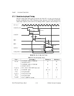
This section includes all of the timing diagrams for the AITM module of the DAQ-STC and
indicates the more common configurations.
2.7.1 Signal Definitions
All timing in this section refers to pin-to-pin timing. Because many of the timing parameter
definitions are based on internal signals and the internal signals can be selected from a variety
of sources, this section defines some global signals that can refer to any one of a number of
pins depending on the internal selection.
Some of the tables in this section indicate that the OSC pin is the reference pin, with
RTSI_OSC immediately following. This means that you can use RTSI_Clock_Mode to
choose between OSC and RTSI_OSC as the reference pin.
2.7.1.1 CONVERT_SRC
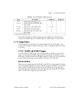
CONVERT_SRC is the signal that causes a CONVERT to be generated. Table 2-2 indicates
the pin selected as CONVERT_SRC based on internal selection.
Table 2-2.
CONVERT_SRC Reference Pin Selection
AI_CONVERT_Source_Select
Reference Pin
0
The CONVERT source is selected to be SI2_TC inverted. The
reference pin is determined by AI_SI2_Source_Select. If
AI_SI2_Source_Select is 0, the reference pin is determined by
AI_SI_Source_Select. If AI_SI2_Source_Select is 1, the
reference pin is OSC or RTSI_OSC, depending on which clock
mode you choose in RTSI_Clock_Mode.
1–10
PFI<0..9>

