14
|
ni.com
|
NI 5782R User Manual and Specifications
6.
LabVIEW generates a preview of your project. Verify that the project is correct and select
Finish
. The new project opens in the
Project Explorer
window.
Creating an FPGA Target VI
1.
Right-click
FPGA Target (RIO
x
, PXI-79
xx
R)
and select
New»FPGA Base Clock
.
2.
In the
Resource
pull-down menu, select
200 MHz Clock
and click
OK
.
3.
Right-click
IO Module
(5782)
in the
Project Explorer
window and select
Properties
.
4.
In the
Clock Selections
category, select
200 MHz Clock
from the pull-down menu for
Clk200
. Leave
Clk40
configured as the
Top-Level Clock
.
5.
Select
NI 5782 CLIP
in the
Name
list of the
Component Level IP
pane.
6.
In the
Clock Selections
category, select
200 MHz Clock
from the pull-down menu for
Clk200
. Leave
Clk40
configured as the
Top-Level Clock
.
7.
Click
OK
.
Note
Configuring these clocks is required for proper CLIP operation. Refer to the
NI 5782 CLIP topics in the
NI FlexRIO Help
for more information about configuring
your clocks.
8.
In the
Project Explorer
window, right-click the FPGA target and select
New»VI
to open
a blank VI.
9.
Select
Window»Show Block Diagram
to open the VI block diagram.
10. In the
Project Explorer
window, expand the
IO Module (NI 5782 : NI 5782)
tree view.
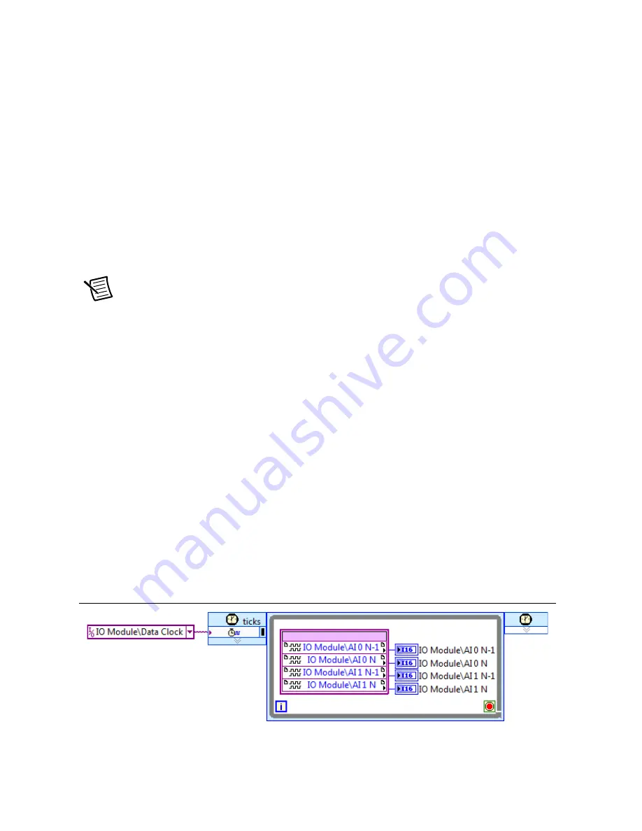
11. Drag
AI 0 Data N-1
to the block diagram.
12. Click and drag the bottom edge of the control node to expose the other signals,
AI 0
N-1
...
AI 1 N.
13. Add a Timed Loop structure around the node.
14. Wire indicators to each output terminal of the
IO Module\AI 0 N-1
...
AI 1 N.
15. Right-click the input node of the Timed Loop to wire an FPGA Clock Constant to the node.
Set this constant to
IO Module\Data Clock
.
Your block diagram should resemble the block diagram in Figure 6.
Figure 6.
5782SampleAcq (FPGA).vi Block Diagram


