


5
5
4
4
3
3
2
2
1
1
D
D
C
C
B
B
A
A
a1
b1
c1
d1
e1
f1
g1
GT1
GT2
GT3
GT1
GT2
GT3
h2
a1
b1
c1
d1
e1
f1
g1
PM
a1
b1
c1
d1
e1
f1
g1
a1
b1
c1
d1
e1
f1
g1
a2
b2
c2
d2
e2
f2
g2
h2
a2
b2
c2
d2
e2
f2
g2
h2
a2
b2
c2
d2
e2
f2
g2
a2
b2
c2
d2
e2
f2
g2
h2
AM
PM
GT3
GT2
GT1
AM
STR
CLK
DTA
BLK
FIL+
DCF
BLK
DTA
CLK
STR
FIL-
TP
DCF
PWM
SEN
PWM
SEN
FIL-
FIL+
TP
5V
5V
HV
5V
5V
5V
5V
5V
5V
HV
5V
5V
5V
5V
Title
Size
Document Number
Rev
Date:
Sheet
of
by. Mr.Nixie, valid from Serial VR-001
10.12
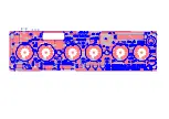
IV-11 VFD-Clock JENNY Reloaded
1
1
Monday, November 26, 2012
Title
Size
Document Number
Rev
Date:
Sheet
of
by. Mr.Nixie, valid from Serial VR-001
10.12
IV-11 VFD-Clock JENNY Reloaded
1
1
Monday, November 26, 2012
Title
Size
Document Number
Rev
Date:
Sheet
of
by. Mr.Nixie, valid from Serial VR-001
10.12
IV-11 VFD-Clock JENNY Reloaded
1
1
Monday, November 26, 2012
Antenna Track 17.4 mm
BU1
USB-Power
16V
16V
16V
25V
25V
16V
OPT
IONAL
low ESR
R14 auf Lötseite bestücken
Solder R14 on bottom side
Siehe Bauanleitung
Please read manual
RN4A
RN4A
DQ
DQ
A
A
LED3 RGB
LED3 RGB
R
G
B
A
R4
22k
R4
22k
SND1
Sounder
SND1
Sounder
IC6
PIC16F1936_IV-11
IC6
PIC16F1936_IV-11
MCLR
1
HV SENSE
2
A1
28
LED B
27
LED G
26
LED R
25
A3
7
VSS
8
LED AM
9
LED PM
10
XTAL1/TCXO
11
XTAL2
12
HV PWM
13
LED DST
14
LED ALARM
15
LED DCF/GPS
16
SOUNDER
17
DCF/GPS
18
VSS
19
VDD
20
SET
21
ADJ
22
ALARM
23
DST
24
DTA
3
CLK
4
STR
5
A2
6
a
b
c
d
e
f
g
h
H4
IV-11
a
b
c
d
e
f
g
h
H4
IV-11
G
2
c
3
g
7
b
5
FI
1
h
4
a
6
f
8
e
9
d
10
FI
11
LED2 RGB
LED2 RGB
R
G
B
A
R12
3k9
R12
3k9
R10
22k
R10
22k
C5
220u
C5
220u
RN1C
RN1C
C22
100u
C22
100u
C1
0u1
C1
0u1
RN5A
RN5A
L4
47uH
L4
47uH
C10
100u
C10
100u
LED1 RGB
LED1 RGB
R
G
B
A
Q1
32kHz
Q1
32kHz
IC2
HV5812
IC2
HV5812
VHV
1
DOUT
2
HV20
3
HV19
4
HV18
5
HV17
6
HV16
7
HV15
8
HV14
9
HV13
10
HV12
11
BLANK
13
GND
14
CLK
15
STROBE
16
HV11
12
HV10
17
HV9
18
HV8
19
HV7
20
HV6
21
HV5
22
HV4
23
HV3
24
HV2
25
HV1
26
VDD
28
DATA
27
R6
22k
R6
22k
C
C
C14
4n7
C14
4n7
RN2C
RN2C
R3
1k
R3
1k
H8
IV-15
H8
IV-15
RN6A
RN6A
R2
22k
R2
22k
J
J
C7
0u1
C7
0u1
RN1A
RN1A
C17
33p
C17
33p
C18
33p
C18
33p
a
b
c
d
e
f
g
h
H5
IV-11
a
b
c
d
e
f
g
h
H5
IV-11
G
2
c
3
g
7
b
5
FI
1
h
4
a
6
f
8
e
9
d
10
FI
11
RN3C
RN3C
D6
1N5819
D6
1N5819
C6
220u
C6
220u
D5
1N5819
D5
1N5819
C11
0u1
C11
0u1
RN1B
RN1B
C4
0.33F
C4
0.33F
II
1
2
3
4
5
R16
22k
R16
22k
H7
IV-15
H7
IV-15
5V
5V
BU2
Time Data
BU2
Time Data
R17
1k
R17
1k
S3
ALARM
S3
ALARM
RN4C
RN4C
DQ
VDD
GND
IC
7
DS18B20
DQ
VDD
GND
IC
7
DS18B20
LED9
SYNC
LED9
SYNC
C19
0u1
C19
0u1
R14
1M
R14
1M
RN2B
RN2B
L2
100uH
L2
100uH
T4
2N7000
T4
2N7000
E
E
C3
100u
C3
100u
a
b
c
d
e
f
g
h
H6
IV-11
a
b
c
d
e
f
g
h
H6
IV-11
G
2
c
3
g
7
b
5
FI
1
h
4
a
6
f
8
e
9
d
10
FI
11
C16
0u1
C16
0u1
R11
3k9
R11
3k9
T1
2N7000
T1
2N7000
R5
47R
R5
47R
LED7
DST
LED7
DST
RN5C
RN5C
C12
100u
C12
100u
a
b
c
d
e
f
g
h
H2
IV-11
a
b
c
d
e
f
g
h
H2
IV-11
G
2
c
3
g
7
b
5
FI
1
h
4
a
6
f
8
e
9
d
10
FI
11
RN3B
RN3B
GND
GND
F
F
T5
2N7000
T5
2N7000
B
B
H
H
RN6C
RN6C
R8
3k9
R8
3k9
a
b
c
d
e
f
g
h
H1
IV-11
a
b
c
d
e
f
g
h
H1
IV-11
G
2
c
3
g
7
b
5
FI
1
h
4
a
6
f
8
e
9
d
10
FI
11
C21
33p
C21
33p
T2
RFD3055L
T2
RFD3055L
R15
47R
R15
47R
RN4B
RN4B
IC1
UCC27524
IC1
UCC27524
ENA
1
INA
2
GND
3
INB
4
OUTB
5
VDD
6
OUTA
7
ENB
8
L1
L1
C2
2200uF
C2
2200uF
T3
2N7000
T3
2N7000
LED10
Data
LED10
Data
S1
SET
S1
SET
C13
0u1
C13
0u1
L3
100uH
L3
100uH
ASK-
RXB2
ASK-
RXB2
GND
SHT
DAT
5V
5V
GND
GND
ANT
RN2A
RN2A
LED6 RGB
LED6 RGB
R
G
B
A
a
b
c
d
e
f
g
h
H3
IV-11
a
b
c
d
e
f
g
h
H3
IV-11
G
2
c
3
g
7
b
5
FI
1
h
4
a
6
f
8
e
9
d
10
FI
11
RN5B
RN5B
C9
0u1
C9
0u1
R13
3k9
R13
3k9
R9
1M
R9
1M
LED5 RGB
LED5 RGB
R
G
B
A
C20
0u1
C20
0u1
G
G
RN3A
RN3A
S4
LED/DST
S4
LED/DST
LED4 RGB
LED4 RGB
R
G
B
A
S2
ADJ
S2
ADJ
RN6B
RN6B
D
D
LED8
ALARM
LED8
ALARM
T6
2N7000
T6
2N7000
R7
1k
R7
1k