background image

- 6 -

BIOS

7h Initialize EISA slot

8h Reserved
9h Calculate total memory by testing the last double last word of each 

6K page; Program writes allocation for AMD K CPU

Ah Reserved

Bh Reserved

Ch Reserved

Dh Reserved

Eh

Program MTRR of M CPU; initialize L2 cache for P6 class CPU & 

program cacheable range; Initialize the APIC for P6 class CPU; On 

MP platform, adjust the cacheable range to smaller one in case the 

cacheable ranges between each CPU are not identical

Fh reserved

0h Initialize USB

h Reserved

2h Test all memory (clear all extended memory to 0)

h Reserved

h Reserved

h Display number of processors (multi-processor platform)

6h Reserved
7h Display PnP logo; Early ISA PnP initialization and assign CSN to 

every ISA PnP device

8h Reserved

9h Initialize the combined Trend Anti-Virus code

Ah Reserved
Bh Show message for entering AWDFLASH.EXE from FDD (optional 

feature)

Ch Reserved
Dh Initialize Init_Onboard_Super_IO switch; Initialize Init_Onboard_

AUDIO switch

Eh Reserved

Fh Reserved

60h Okay to enter Setup utility

6h Reserved

62h Reserved

6h Reserved

6h Reserved

6h Initialize PS/2 mouse

66h Reserved

67h Prepare memory size information for function call: INT h ax=E820h

68h Reserved

69h Turn on L2 cache

6Ah Reserved
6Bh Program chipset registers according to items described in Setup & 

Auto-Configuration table

6Ch Reserved
6Dh Assign resources to all ISA PnP devices; Auto assign ports to onboard 

COM ports if the corresponding item in Setup is set to “AUTO”

6Eh Reserved

6Fh

Initialize floppy controller; Setup floppy related fields in 40:hardware

Summary of Contents for EmCORE-i9457

Page 1: ...EmCORE i9457 3 5 Embedded Board User s Manual Version 1 1 2008 08 ...

Page 2: ...This page is intentionally left blank ...

Page 3: ... 11 1 14 Heatsink Dimensions 12 Chapter 2 Installation 13 2 2 Jumpers and Connectors 15 Jumpers 16 JRS2 COM2 RS 232 422 485 Mode Select 16 LV3 LV4 COM2 Power source Special Support 16 JBAT1 Clear CMOS Setup 17 JVLCD1 LCD Panel Voltage Select 17 Connectors 18 INV1 LCD Inverter Connector 18 SATA1 Serial ATA Connector 18 LPT1 Parallel Port or FDD Connector 19 JFRT1 Switches 20 IDE1 Primary IDE Connec...

Page 4: ...S Introduction 32 3 2 BIOS Setup 32 3 3 Standard CMOS Features 33 3 4 Advance BIOS Features 36 3 5 Advanced Chipset Features 39 3 6 Integrated Peripherals 41 3 7 Power Management Setup 44 3 8 PNP PCI Configurations 46 3 9 PC Health Status 48 3 10 Load Optimized Defaults 49 3 11 Set Password 50 3 12 Save Exit Setup 51 3 13 Exit Without Saving 52 3 14 BIOS Beep Sound code list 53 3 15 BIOS memory ma...

Page 5: ... Introduction 1 Chapter 1 Introduction Chapter 1 Introduction ...

Page 6: ...the manufacturer 1 2 About this User s Manual This User s Manual is intended for experienced users and integrators with hardware knowledge of personal computers If you are not sure about any description in this User s Manual please consult your vendor before further handling 1 3 Warning Single Board Computers and their components contain very delicate Integrated Circuits IC To protect the Single B...

Page 7: ...ufacturer Do not throw lithium batteries into the trashcan It must be disposed of in accordance with local regulations concerning special waste 1 5 Technical Support If you have any technical difficulties please consult the user s manual first at ftp ftp arbor com tw pub manual Please do not hesitate to call or e mail our customer service when you still can not find out the answer http www arbor c...

Page 8: ... use misuse of or inability to use this product Vendor will not be liable for any claim made by any other related party Vendors disclaim all other warranties either expressed or implied including but not limited to implied warranties of merchantibility and fitness for a par ticular purpose with respect to the hardware the accompanying product s manual s and written materials and any accompanying h...

Page 9: ...nector 2x5 pins If any of the above items is damaged or missing contact your vendor immediately 1 8 Ordering Information EmCORE i9457VLG 3 5 Intel 65nm µFC PGA Core Duo Core 2 Duo Celeron M 667MHz Embedded Board with CRT LCD Audio and Gb LAN Cable kit CBK 08 9457 00 1 x Audio Cable 1 x COM Port Cable 1 x LPT to FDD Cable 1 x IDE Cable 1 x LPT Cable 1 x Keyboard mouse Cable 1 x SATA Cable 2 x USB C...

Page 10: ...ND W83627 BIOS Phoenix Award PnP Flash BIOS Audio ALC655 AC 97 Codec Line in out Mic in IDE Interface 1 x IDE Ultra ATA 33 support 2 IDE devices SATA 1 x Serial ATA 300MB s HDD transfer rate Serial Port 2 x COM port 1 x RS232 1x RS232 422 485 selectable Parallel Port Floppy 1 x SPP EPP ECP mode 1 x Floppy connector shared with Parallel Port KBMS Standard PS 2 Keyboard and Mouse Universal Serial Bu...

Page 11: ...n 1 10 Board Dimensions CF 1 mPGA478 SOCKET 10 5 5 6 1 1 1 2 1 30 1 6 5 3 35 28 24 32 64 22 48 14 61 115 11 132 27 67 2 29 47 47 75 42 16 41 28 103 32 29 46 8 84 3 38 95 2 101 96 46 99 3 1 6 3 5 7 59 90 1 6 Unit mm ...

Page 12: ... Introduction 10 5 30 1 3 35 28 24 1 2 29 47 47 75 4 4 8 84 133 93 3 38 95 2 101 96 146 46 99 95 91 31 47 7 59 90 1 6 1 Unit mm ...

Page 13: ...e CPU Place the CPU into the socket by making sure the notch on the corner of the CPU corresponding with the notch on the inside of the socket Once the CPU has slide into the socket lock the screw Make sure that heat sink of the CPU top surface is in complete contact to avoid the CPU overheating problem If not it would cause your system or CPU to be hanged unstable damaged ...

Page 14: ...on 3 Applying the board side notch in parallel to the socket bottom so that the board position cannot be displaced press the board side notch up and fix it to the latch portion at both socket edges Press the board side notch and release the notch with a snap click tone if the printed board exceeds the latch claw head Side notch Key Latch knob Latch claw Latch section Latch arm Polarizing key 1 2 3...

Page 15: ...nd screw it on in the direction of the board Insert four screws No 1 downward into the holes and turn them tightly Verify the direction is correct No 2 and plug the FAN connector into CPUF1 connector 2 1 13 Heatsink Installation FAN Connector 1 1 1 1 2 ...

Page 16: ... 12 Introduction 1 14 Heatsink Dimensions 90 66 20 20 20 20 40 14 5 43 7 10 15 75 12 5 7 17 9 18 3 25 30 25 9 5 ...

Page 17: ... 13 Installation 2 Chapter 2 Installation Chapter 2 Installation ...

Page 18: ...l CPU PCIe LAN Controller FSB 667 533MHz DMI I F USB I F Serial ATA I F IDE ATA I F Intel ICH7M 1 x IDE 1 x CF 6 x USB 1 x SATA Audio Memory Bus Super IO COM1 COM2 LPT1 FDD KB MS Codec AC 97 LPC I F 1 x LAN RJ 45 1 x 200 pin DDRII SO DIMM socket PCIe Bus LVDS LVDS PCI Bus 1 x MiniPCI Socket ...

Page 19: ...19 20 2 1 1 29 30 2 9 10 10 1 2 9 1 2 1 1 1 2 9 10 2 5 5 0 2 6 1 2 0 0 1 9 9 2 1 4 0 4 2 3 9 4 1 JVLCD1 CPUF1 ATX1 LVDS1 LED1 COM1 VGA1 JBAT1 RES1 KBM1 MINIPCI1 LAN1 USB1 AUDIO1 COM2 IDE1 JFRT1 LPT1 SATA1 INV1 DIMM1 JV3 JV4 JCOM2 JRS2 JSMB1 CFD1 USB2 USB3 1 2 3 4 6 7 8 5 9 10 14 13 26 15 11 12 17 18 19 20 21 22 23 24 25 16 1 ...

Page 20: ...et All RS 232 422 482 modes are available on COM2 It can be configured COM2 to operate in RS 232 RS 422 or RS 485 mode Connector type 2 00mm pitch 2x3 pin header Mode RS 232 Default RS 422 RS 485 1 2 ON OFF OFF 3 4 OFF ON OFF 5 6 OFF OFF ON 6 5 2 1 6 5 2 1 6 5 2 1 LV3 LV4 COM2 Power source Special Support 14 15 The voltage of COM2 could be selected by LV3 and LV4 to 5V or 12V Connector type 2 54mm...

Page 21: ...ting Solution A 1 Power off the system and disconnect the power cable 2 Place a shunt to short pin 1 and pin 2 of JBAT1 for five seconds 3 Place the shunt back to pin 2 and pin 3 of JBAT1 4 Power on the system Solution B If the CPU Clock setup is incorrect you may not be able to boot up In this case follow these instructions 1 Turn the system off then on again The CPU will automatically boot up us...

Page 22: ...ess control 5 GND SATA1 Serial ATA Connector 2 The EmCORE i9457 CPU board on board supports four SATA II connectors second generation SATA drives transfer data at speeds as high as 300MB s twice the transfer speed of first generation SATA drives The SATA drives can be configured in a RAID 0 RAID 1 or RAID 10 configuration Pin Description 1 7 1 GND 2 TX 3 TX 4 GND 5 RX 6 RX 7 GND ...

Page 23: ...or floppy disk drive interface through BIOS setup Pin Description Pin Description 1 N C 2 RWC 3 RINDEX 4 HEAD 5 TRAK0 6 DIR 7 WP 8 STEP 9 RDATA 10 GND 11 DSKCHG 12 GND 13 N C 14 N C 15 N C 16 MOB 17 N C 18 WD 19 DSB 20 WE BIOS Setup The default is to set LPT1 as FDD connector To change the value get into BIOS setup Integrated Peripheral Super IO Device BIOS Option Setting Description External FDD ...

Page 24: ...e 2 54 mm pitch 2x2 pin header Pin Description Pin Description 1 2 3 4 1 PWRBTN 2 PWRBTN 3 RST 4 RST PWRBTN ATX soft power switch pin 1 2 This 2 pin connector connects to the case mounted Power button RES Reset Button pin 3 4 This 2 pin connector connects to the case mounted reset switch and is used to reboot the system ...

Page 25: ... settings You must orient the cable connector so that the pin 1 color edge of the cable corresponds to pin 1 of the IDE connector Connector type 2 0mm pitch 2x22 box header Pin Description Pin Description 1 2 43 44 1 IDE RESET 2 GND 3 DATA7 4 DATA8 5 DATA6 6 DATA9 7 DATA5 8 DATA10 9 DATA4 10 DATA11 11 DATA3 12 DATA12 13 DATA2 14 DATA13 15 DATA1 16 DATA14 17 DATA0 18 DATA15 19 GND 20 N C Key 21 REQ...

Page 26: ... 1 5MB s USB devices Connector type 2 00mm 2x5 pin header Pin Description Pin Description 1 2 10 9 1 5V 2 5V 3 USBD1 4 USBD2 5 USBD1 6 USBD2 7 GND 8 GND 9 GND 10 N C Key JSMB1 External SMBUS Connector 8 Connector type 2 00mm pitch 1x3 box wafer connector Pin Description 1 2 3 1 Data 2 Clock 3 GND JCOM2 RS 422 485 Output Connector 10 Connector type 2 00mm pitch 1x4 box wafer connector Pin RS 422 RS...

Page 27: ...nother audio source to the light blue Line in connector to record audio on your computer or to play audio through your computer s sound chip and speakers Connect a micro phone to the pink microphone connector to record audio to your computer Connector type 2 00mm pitch 2x5 pin header Pin Description Pin Description 10 9 1 2 1 Line in Left 2 Line in Right 3 GND 4 GND 5 MIC1 6 MIC2 7 GND 8 GND 9 Lin...

Page 28: ...nnector 17 LAN1 supports one 10 100 1000 base T Ethernet Connector type RJ 45 LED LED LAN USB USB 8 7 6 5 4 3 2 1 1 2 3 4 1 2 3 4 KBM1 Keyboard Mouse 18 Mini Din Keyboard Mouse connector Pin Description 1 2 3 5 6 4 1 KB Data 2 MS Data 3 GND 4 5V 5 KB Clock 6 MS Clock Note KBM1 supports PS 2 keyboard directly and PS 2 mouse supported with the additional PS 2 1 to 2 cable in standard packing ...

Page 29: ...on Pin Description 1 5 15 11 1 RED 9 5V VCC 2 GREEN 10 GND 3 BLUE 11 N C 4 N C 12 D DATA 5 GND 13 HSYNC 6 GND 14 VSYNC 7 GND 15 D DCLK 8 GND COM1 RS232 Connector 21 Connector type D Sub 9 pin male Pin Description Pin Description 1 5 9 6 1 DCD 6 DSR 2 RXD 7 RTS 3 TXD 8 CTS 4 DTR 9 RI 5 GND ...

Page 30: ...nto the connector Pin Description Pin Description 1 6 5 10 6 5VSB 1 PS ON 7 5V 2 GND 8 5V 3 GND 9 N C 4 12V 10 GND 5 3 3V Warning Incorrect installation of the power supply could result in serious damage to the mainboard and connected peripherals Make sure the power supply is unplugged from the AC outlet before connecting the leads from the power supply CPUF1 CPU Fan Power Connector 24 CPUF1 is 3 ...

Page 31: ...V or 3 3V Connector type DF 13 30DP 1 25V Pin Description Pin Description 1 29 30 2 2 VDD 1 VDD 4 TX2CLK 3 TX1CLK 6 TX2CLK 5 TX1CLK 8 GND 7 GND 10 TX2D0 9 TX1D0 12 TX2D0 11 TX1D0 14 GND 13 GND 16 TX2D1 15 TX1D1 18 TX2D1 17 TX1D1 20 GND 19 GND 22 TX2D2 21 TX1D2 24 TX2D2 23 TX1D2 26 GND 25 GND 28 TX2D3 27 TX1D3 30 TX2D3 29 TX1D3 ...

Page 32: ...40 N C 16 GND 41 IDERST 17 GND 42 PIORDY 18 PDA2 43 PDDREQ 19 PDA1 44 PDDACK 20 PDA0 45 HD_LED1 21 PDD0 46 PDIAG 22 PD1 47 PDD8 23 PD2 48 PDD9 24 N C 49 PDD10 25 N C 50 GND The interface of Compact Flash socket is designated to use IDE1 Installation instructions Compact Flash CF card is not hot swap If the CF card is swapped in the condition of system power on it will damage the CF card Make sure ...

Page 33: ...29 Installation 2 3 The Installation Paths of CD Driver Driver Path AUDIO AUDIO REALTEK_AC97 WINDOWS_A401 CHIPSET CHIPSET INTEL INF 8 1 LAN ETHERNET REALTEK 8111B_WIN5640 VGA GRAPHICS INTEL_2K_XP_32 1431 ...

Page 34: ... 30 Installation This page is intentionally left blank ...

Page 35: ... 31 BIOS 3 Chapter 3 BIOS Chapter 3 BIOS ...

Page 36: ...te keys You can also restart by turning the system Off and back On again The following message will appear on the screen Press DEL to Enter Setup In general you press the arrow keys to highlight items Enter to select the PgUp and PgDn keys to change entries F1 for help and Esc to quit When you enter the Setup utility the Main Menu screen will appear on the screen The Main Menu allows you to select...

Page 37: ...t this option You will need to run the Standard CMOS option however if you change your system hardware configurations such as onboard battery fails or the configuration stored in the CMOS memory was lost or damaged Date The date format is Day Sun to Sat Month 1 to 12 Date 1 to 31 Year 1999 to 2099 Time The time format is Hour 00 to 23 Minute 00 to 59 Second 00 to 59 To set the date time highlight ...

Page 38: ... Precomp Write precompensation Landing Zone Landing zone Sector Number of sectors The Access Mode selections are as follows CHS HD 528MB LBA HD 528MB and supports Logical Block Addressing Large for MS DOS only Auto Drive A These fields identify the types of floppy disk drive A that has been installed in the computer The available specifications are None 360K 5 25 in 1 2M 5 25 in 720K 3 5 in 1 44M ...

Page 39: ...mpted No errors default The system boot will not be halted for any error that may be detected All But Keyboard The system boot will not be halted for a keyboard error it will stop for all other errors All But Diskette The system boot will not be halted for a disk error it will stop for all other errors All But Disk Key The system boot will not be halted for a keyboard or disk error it will stop fo...

Page 40: ...as well as the Bootable Add in Card that is relevant to other boot sources media such as SCSI cards and LAN cards Hyper Threading Technology If enabled when your processor supports Hyper Threading Technology Quick Power On Self Test When enabled it speeds up the Power On Self Test POST after the system is turned on If it is set to Enabled BIOS will skip some items Setting Disabled Enabled Default ...

Page 41: ...e system to search for an OS from other devices other than the ones selected in the First Second Third Boot Device Setting Disabled Enabled Default First Second Boot Device These fields determine the drive that the system searches first for an operating system The options available include Setting Floppy Hard Disk CDROM USB FDD USB ZIP USB CDROM LAN and Disabled ...

Page 42: ...ord every time you boot up When you select Setup the system always boots up and prompts for the Supervisor Password only when the Setup utility is called up Setting Setup Default System APIC Mode APIC stands for Advanced Programmable Interrupt Controller Setting Disabled Enabled Default EEPROM Write Protect Setting Disabled Enabled Default ...

Page 43: ...Onchip VGA PEG Port Auto Default On Chip Frame Buffer Size Setting 1MB 8MB Default PEG Force X1 Setting Disabled Default Enabled DVMT FIXED Memory Size Setting 64MB 128MB Default 224MB DVMT Mode Setting FIXED DVMT Default Both Boot Display Setting CRT LCD CRT LCD Default ...

Page 44: ... 40 BIOS Panel Number It allows you to select the LCD Panel type as below Setting 640x480 800x600 1024x768 Default 1280x768 1400x1050 1400x1050 1600x1200 1280x768 1680x1050 1920x1200 ...

Page 45: ...lock mode to transfer data to and from HDD Setting Disabled Enabled Default On Chip Primary PCI IDE The integrated peripheral controller contains an IDE interface with support for two IDE channels Select Enabled to activate each channel separately Setting Disabled Enabled Default OnChip IDE Device ...

Page 46: ...e Setting Auto Default Mode 0 Mode 1 Mode 2 Mode 3 Mode 4 IDE Primary Master Slave UDMA It allows your system to improve disk I O throughput to 33MB sec with the Ultra DMA33 feature Setting Disabled Auto USB Controller Setting Enabled Default Disabled Onboard Device USB 2 0 Controller For using USB 2 0 it is necessary OS drivers must be installed first Please update your system to at least Windows...

Page 47: ...ult Parallel Port 378 IRQ7 Default Onboard FDC Controller Select Enabled if your system has a floppy disk controller FDC installed and you wish to use it Select Disabled if your system has an add in FDC or has no floppy drive Setting Disabled Enabled Default Parallel Port Mode Setting SPP Default EPP ECP ECP EPP Normal EPP Mode Select Setting EPP1 9 EPP1 7 Default ECP Mode Use DMA Setting 1 3 Defa...

Page 48: ... HDD Power Down which ranges from 1 min to 15 min Min Saving Minimum power management Max Saving Maximum power management Video Off Method It defines the Video Off features Setting Blank Screen Writes blanks to the video buffer V H SYNC Blank blank the screen and turn off vertical and horizontal scanning DPMS Default Allowing BIOS to control the video display Video Off In Suspend When enabled the ...

Page 49: ...N After PWR Fail It sets the system power status whether on or off when power returns to the system from a power failure situation Setting Off Default On Former Sts Power On by Ring It enables or disables the power on of the system through the modem connected or LAN Setting Disabled Default Enabled Resume by Alarm It enables or disables the resumption of the system operation When enabled the user ...

Page 50: ... Reset Configuration Data It allows you to determine whether to reset the configuration data or not Setting Disabled Default Enabled Resources Controlled By This PnP BIOS can configure all of the boot and compatible devices with the use of a PnP operating system Setting Auto ESCD Default Manual ...

Page 51: ...n Enabled a PCI VGA can display with an MPEG ISA VESA VGA card When Disabled a PCI VGA cannot display with an MPEG ISA VESA VGA card Setting Disabled Default Enabled INT Pin 1 8 Assignment Setting Auto Default 3 4 5 7 9 10 11 12 14 15 Maximum Payload Size It allows you to set maximum TLP payload size for PCI Express devices The unit is byte Setting 128 256 512 1024 2048 4096 Default ...

Page 52: ... 48 BIOS 3 9 PC Health Status Current System Temperature Current System FAN Current CPU FAN Vcore Current CPU Temperature ...

Page 53: ... 49 BIOS 3 10 Load Optimized Defaults It allows you to load the default values to your system configuration The default setting is optimal and enabled all high performance features ...

Page 54: ...ssword up to eight characters in length and press Enter And the system confirms your password by asking you to type it again After setting a password the screen automatically returns to the main screen To disable a password just press the Enter key when you are prompted to enter the password A message will confirm the password to be disabled Once the password is disabled the system will boot then ...

Page 55: ... 51 BIOS 3 12 Save Exit Setup Typing Y you will quit the setup utility and save all the changes into the CMOS memory Typing N you will return to Setup utility ...

Page 56: ... 52 BIOS Typing Y will quit the Setup utility without saving the modifications Typing N will return you to Setup utility 3 13 Exit Without Saving ...

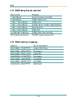
Page 57: ... short Beep Keyboard error 1 long 9 short Beep ROM error Long Beep continuous DRAM hasn t inset correctly Short Beep continuous POWER supply has problem Address Device Description E000 0000h F000 FFFFh System BIOS Area D000 2000h D000 FFFFh Free space D000 0000h D000 1FFFh LAN ROM C000 E000h CF00 FFFFh Free space C000 0000h C000 DFFFh VGA BIOS A000 0000h B000 FFFFh VGA RAM 0000 0000h 9000 FFFFh DO...

Page 58: ...p optional Reset keyboard for Winbond 977 series Super I O chips 0Bh Reserved 0Ch Reserved 0Dh Reserved 0Eh Test F000h segment shadow to see whether it is read write capable or not If test fails keep beeping the speaker 0Fh Reserved 10h Auto detect flash type to load appropriate flash read write codes into the run time area in F000 for ESCD DMI support 11h Reserved 12h Use walking 1 s algorithm to...

Page 59: ...fer 28h Reserved 29h Program CPU internal MTRR P6 PII for 0 640K memory address Initialize the APIC for Pentium class CPU Program early chipset according to CMOS setup Measure CPU speed Invoke video BIOS 2Ah Reserved 2Bh Reserved 2Ch Reserved 2Dh Initialize multilanguage Put information on screen display including Award title CPU type CPU speed etc 2Eh Reserved 2Fh Reserved 30h Reserved 31h Reserv...

Page 60: ...PnP initialization and assign CSN to every ISA PnP device 58h Reserved 59h Initialize the combined Trend Anti Virus code 5Ah Reserved 5Bh Show message for entering AWDFLASH EXE from FDD optional feature 5Ch Reserved 5Dh Initialize Init_Onboard_Super_IO switch Initialize Init_Onboard_ AUDIO switch 5Eh Reserved 5Fh Reserved 60h Okay to enter Setup utility 61h Reserved 62h Reserved 63h Reserved 64h R...

Page 61: ... is set ask for password 83H Save all data in stack back to CMOS 84h Initialize ISA PnP boot devices 85h Final USB initialization NET PC Build SYSID structure Switch screen back to text mode Set up ACPI table at top of memory Invoke ISA adapter ROM s Assign IRQ s to PCI devices Initialize APM Clear noise of IRQ s 86h Reserved 87h Reserved 88h Reserved 89h Reserved 90h Reserved 91h Reserved 92h Res...

Page 62: ... 58 BIOS This page is intentionally left blank ...

Page 63: ... 59 Appendix 4 Chapter 4 Appendix Chapter 4 Appendix ...

Page 64: ...dary IDE Channel 000001F0 000001F7 Primary IDE Channel 00000274 00000277 ISAPNP Read Data Port 00000279 00000279 ISAPNP Read Data Port 000002F8 000002FF Communications Port 00000378 0000037F Printer Port 000003B0 000003BB Intel R 82945G Express Chipset Family 000003C0 000003DF Intel R 82945G Express Chipset Family 000003F0 000003F5 Standard floppy disk controller 000003F6 000003F6 Primary IDE Chan...

Page 65: ...0 0000FA3F Realtek AC 97 Audio 0000FB00 0000FB1F Intel R 82801G ICH7 Family USB Universal Host Controller 27CB 0000FC00 0000FC1F Intel R 82801G ICH7 Family USB Universal Host Controller 27CA 0000FC00 0000FC1F Intel R 82801G ICH7 Family USB Universal Host Controller 27C9 0000FE00 0000FE1F Intel R 82801G ICH7 Family USB Universal Host Controller 27C8 0000FF00 0000FF07 Mobile Intel R 945GM Express Ch...

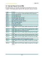
Page 66: ...S 2 Compatible Mouse IRQ 14 Primary IDE Channel IRQ 15 Secondary IDE Channel IRQ 16 Intel R 82801G ICH7 Family USB Universal Host Controller 27CB IRQ 16 Intel R 82801G ICH7 Family PCI Express Root Port 27D0 IRQ 16 Intel R 82945G Express Chipset Family IRQ 18 Intel R 82801G ICH7 Family USB Universal Host Controller 27CA IRQ 19 Intel R 82801G ICH7 Family PCI Express Root Port 27D6 IRQ 19 Intel R 828...

Page 67: ...it Ethernet NIC FDB00000 FDBFFFFF Intel R 82801G ICH7 Family PCI Express Root Port 27D0 FDE00000 FDEFFFFF Intel R 82801G ICH7 Family PCI Express Root Port 27D0 FDF00000 FDF7FFFF Mobile Intel R 945GM Express Chipset Family FDF80000 FDFBFFFF Mobile Intel R 945GM Express Chipset Family FDFFD000 FDFFD0FF Realtek AC 97 Audio FDFFE000 FDFFE1FF Realtek AC 97 Audio FDFFF000 FDFFF3FF Intel R 82801G ICH7 Fa...

Page 68: ... 64 Appendix ...

Reviews: