background image

2-6

Computer Group Literature Center Web Site

Functional Description

2

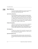
Super I/O Device

The VP22 uses the Super I/O (SIO) device to provide two asynchronous 
serial ports, a peripheral parallel port, a PS/2 floppy port, PS/2 
keyboard/mouse ports and an IrDA header.

Asynchronous Serial Ports

Two 16550-compatible asynchronous serial ports are supported on the 
VP22 motherboard. The EIA-232 drivers and receivers reside onboard. 
COM1 is routed to an industry-standard DB-9 connector accessible from 
the rear panel and COM2 is routed to an optional 10-pin header. Both ports 
are configured as DTE. Maximum data rate on any port is 115.2K baud.

Firmware initializes the two serial ports as COM1 and COM2 with ISA I/O 
base addresses of 3F8h and 2F8h respectively. This default configuration 
also assigns COM1 to IRQ4 and COM2 to IRQ3.  

Peripheral Parallel Port

All parallel I/O interface signals are routed to an industry-standard DB-25 
connector, accessible from the rear panel. This port supports the full 
IEEE-1284 capability, which provides the basic printer interface. 
Firmware initializes the parallel port as LPT1 with ISA I/O base address of 
378h. This default configuration also assigns the parallel port to IRQ7. 

PS/2 Floppy Port

The floppy port is configured for PS/2 compatibility and supports both the 
legacy 34-pin header and the compact floppy disk drive (FDD) connector. 
Up to two floppy drives are supported.

Keyboard and Mouse Ports

Two 6-pin circular DIN connectors are located on the rear panel of the 
VP22 motherboard for the keyboard and mouse connections. The power 
provided to the keyboard and mouse is protected by a polyswitch rated at 
1.1 A.

Summary of Contents for VP22A/IH1

Page 1: ...VP22 microATX Motherboard Installation and Use VP22A IH1 June 2001 Edition ...

Page 2: ...istered trademark and Celeron is a trademark of Intel Corporation VxWorks is a registered trademark of Wind River Systems Inc Linux is a registered trademark of Linus Torvalds Windows and Windows NT are registered trademarks of Microsoft in the U S and other countries All other products mentioned in this document are trademarks or registered trademarks of their respective holders ...

Page 3: ...the Equipment Operating personnel must not remove equipment covers Only Factory Authorized Service Personnel or other qualified service personnel may remove equipment covers for internal subassembly or component replacement or any internal adjustment Service personnel should not replace components with power cable connected Under certain conditions dangerous voltages may exist even with the power ...

Page 4: ...losion if battery is replaced incorrectly Replace battery only with the same or equivalent type recommended by the equipment manufacturer Dispose of used batteries according to the manufacturer s instructions Attention Caution Il y a danger d explosion s il y a remplacement incorrect de la batterie Remplacer uniquement avec une batterie du même type ou d un type équivalent recommandé par le constr...

Page 5: ...rts have been made to assure the accuracy of this document Motorola Inc assumes no liability resulting from any omissions in this document or from the use of the information obtained therein Motorola reserves the right to revise this document and to make changes from time to time in the content hereof without obligation of Motorola to notify any person of such revision or changes Electronic versio...

Page 6: ...d to in writing by Motorola Inc Use duplication or disclosure by the Government is subject to restrictions as set forth in subparagraph b 3 of the Rights in Technical Data clause at DFARS 252 227 7013 Nov 1995 and of the Rights in Noncommercial Computer Software and Documentation clause at DFARS 252 227 7014 Jun 1995 Motorola Inc Computer Group 2900 South Diablo Way Tempe Arizona 85282 ...

Page 7: ...ation Preliminaries 1 6 VP22 Motherboard Installation 1 7 DIMM Memory Installation 1 8 PCI Adapter Board Installation Optional 1 9 Connection to Peripherals 1 11 Completing the Installation 1 13 Processor Removal and Replacement 1 13 Replacing Lithium Batteries 1 14 CHAPTER 2 Functional Description Introduction 2 1 Features 2 2 General Description 2 3 VP22 Processor 2 4 System Memory 2 4 L2 Cache ...

Page 8: ...dog Timer 2 9 CHAPTER 3 Connector Pin Assignments Connector Pin Assignments 3 1 APPENDIX A Specifications Specifications A 1 APPENDIX B Thermal Analysis Thermally Significant Components B 1 Component Temperature Measurement B 3 Preparation B 3 Measuring Junction Temperature B 4 Measuring Case Temperature B 4 Measuring Local Air Temperature B 6 APPENDIX C Related Documentation Motorola Computer Gro...

Page 9: ...ard Layout 1 4 Figure 2 1 VP22 Block Diagram 2 1 Figure B 1 Thermally Significant Components Primary Side B 3 Figure B 2 Mounting a Thermocouple Under a Heatsink B 5 Figure B 3 Measuring Local Air Temperature B 6 List of Figures ...

Page 10: ......

Page 11: ... 3 11 ATX Power Connector CN11 3 5 Table 3 12 Floppy Disk Drive Connector CN12 3 6 Table 3 13 IrDA Connector CN13 3 6 Table 3 14 Front Panel Connector CN14 3 7 Table 3 15 Open Chassis Alarm Connector CN15 3 8 Table 3 16 Compact Floppy Disk Drive Connector CN16 3 8 Table 3 17 Internal USB 2 Connector CN17 3 9 Table 3 18 CPU Fan Connector FN1 3 9 Table 3 19 Chassis Fan Connector FN2 3 9 Table 3 20 S...

Page 12: ......

Page 13: ...ers listed in the following table Overview of Contents This manual is divided into the following chapters and appendices Chapter 1 Hardware Preparation and Installation provides information on hardware preparation and installation for the VP22 motherboard Chapter 2 Functional Description describes the VP22 motherboard computer on a block diagram level Model Number Description All models include Et...

Page 14: ...all documentation related to the VP22 motherboard Comments and Suggestions Motorola welcomes and appreciates your comments on its documentation We want to know what you think about our manuals and how we can make them better Mail comments to Motorola Computer Group Reader Comments DW164 2900 S Diablo Way Tempe Arizona 85282 You can also submit comments to the following e mail address reader commen...

Page 15: ...and files italic is used for names of variables to which you assign values Italic is also used for comments in screen displays and examples and to introduce new terms courier is used for system output for example screen displays reports examples and system prompts Enter Return or CR represents the carriage return or Enter key Ctrl represents the Control key Execute control characters by pressing t...

Page 16: ......

Page 17: ...el 815E chipset with support for 66 100 133 processor side bus 256MB of L2 cache Pentium III 128MB of L2 cache Celeron Three 168 pin DIMM sockets for 32MB to 512MB PC133 SDRAM Four 32 bit 33 MHz PCI expansion slots One 10BaseT 100BaseTX Ethernet port Two EIDE Ultra DMA 100 hard drive ports Video and audio interfaces Two asynchronous serial ports One peripheral parallel port Floppy port keyboard po...

Page 18: ... 2 Configure the hardware by setting jumpers on the motherboard VP22 Motherboard Preparation on page 1 3 Install the motherboard in the chassis VP22 Motherboard Installation on page 1 7 Ensure that DIMM memory module s are properly installed on the motherboard DIMM Memory Installation on page 1 8 If applicable install a PCI adapter board on the motherboard PCI Adapter Board Installation Optional o...

Page 19: ...ovides software control over all but one option CMOS clear This option is controlled through the manual installation or removal of a header jumper VP22 Motherboard Preparation Figure 1 1 illustrates the placement of the header connectors and various other components on the VP22 motherboard The only manually configurable header on the motherboard is listed in Table 1 2 The header s default setting ...

Page 20: ...and Installation 1 Figure 1 1 VP22 Motherboard Layout PCI 4 CN3 CN4 U9 U14 PCI 3 PCI 2 PCI 1 PH1 PH2 PH3 BT1 CN6 CN7 O1 O3 L23 L22 O1 U6 U7 X1 X2 DIMM1 DIMM2 DIMM3 X4 U16 BZ1 JP1 CN9 CN15 FN1 FN2 FN3 CN13 CN14 CN17 CN16 CN8 CN10 CN12 U15 U13 CN11 Q5 U10 CN5 CN2 CN1 U1 ...

Page 21: ...d You forgot the supervisor or user password You are unable to boot up the computer system because the processor s clock ratio was incorrectly set in the BIOS To load the default values stored in the ROM BIOS follow the steps below 1 Power off the system 2 Remove jumper from JP1 pins 1 2 and put on JP1 pins 2 3 Wait for a few seconds and set JP1 back to its default setting pins 1 2 3 Power on the ...

Page 22: ...ng a system Electronic components such as disk drives computer boards and memory modules can be extremely sensitive to electrostatic discharge ESD After removing the component from its protective wrapper or from the system place the component flat on a grounded static free surface and in the case of a board component side up Do not slide the component over any surface If an ESD station is not avai...

Page 23: ...result in damage to module components Warning Warning Dangerous voltages capable of causing death are present in this equipment Use extreme caution when handling testing and adjusting 3 Remove the chassis cover If necessary loosen or temporarily remove chassis components power supply fans etc as needed for access to the interior of the chassis 4 Install metal standoffs on the floor of the chassis ...

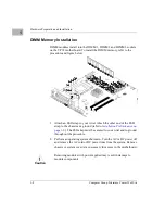
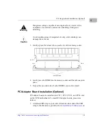
Page 24: ... wrist Attach the other end of the ESD strap to the chassis as a ground refer to Installation Preliminaries on page 1 6 The ESD strap must be secured to your wrist and to ground throughout the procedure 2 Perform an operating system shutdown Turn the AC or DC power off and remove the AC cord or DC power lines from the system Remove chassis or system cover s as necessary for access to the motherboa...

Page 25: ...ad the release tabs on each side of the memory socket 4 Gently press the DIMM into the memory socket until the tabs snap into place 5 Repeat this procedure for all other DIMMs you want to install PCI Adapter Board Installation Optional PCI adapter boards are installed into PCI 1 PCI 2 PCI 3 and PCI 4 slots on the VP22 motherboard To install PCI adapter boards proceed as follows 1 Attach an ESD str...

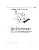
Page 26: ...from the system Remove chassis or system cover s as necessary for access to the motherboard Caution Caution Inserting or removing modules with power applied may result in damage to module components Warning Warning Dangerous voltages capable of causing death are present in this equipment Use extreme caution when handling testing and adjusting Caution Caution Avoid touching areas of integrated circ...

Page 27: ...slots Connection to Peripherals When the VP22 motherboard is installed in a chassis and modules are installed on the VP22 you are ready to connect peripherals and apply power to the board Figure 1 1 on page 1 4 shows the locations of the various cable connectors They are also listed in Table 1 3 with the rest of the connectors ...

Page 28: ... Bus USB panel connectors Ethernet panel connector PH1 Audio MIC IN panel connector PH2 Audio LINE IN panel connector PH3 Audio LINE OUT panel connector Board Surface Connectors CN6 CD IN board connector CN7 COM2 serial board connector CN8 Secondary IDE board connector CN9 Temperature sensor board connector CN10 Primary IDE board connector CN11 ATX power board connector CN12 Floppy disk drive boar...

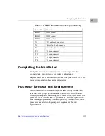
Page 29: ...to ensure proper operation under board specific BIOS software within specified power and cooling requirements Field replacement of the processor is not recommended A processor of a different type or with a different stepping mask may not be supported by the BIOS Also faster processors may alter cooling and power requirements beyond specifications DIMM 1 DIMM socket DIMM 2 DIMM socket DIMM 3 DIMM s...

Page 30: ...tery observe the following guidelines and follow the steps below Note When replacing the battery power must be applied to the board to prevent data loss Warning Warning To prevent serious injury or death from dangerous voltages use extreme caution when handling testing and adjusting this equipment and its components Warning Warning Lithium batteries incorporate flammable materials such as lithium ...

Page 31: ...cuits Use ESD Wrist Strap ESD Attach an ESD strap to your wrist Attach the other end of the ESD strap to an electrical ground Note that the system chassis may not be grounded if it is unplugged The ESD strap must be secured to your wrist and to ground throughout the procedure 1 To remove the battery from the module carefully pull the battery from the socket 2 Before installing a new battery ensure...

Page 32: ......

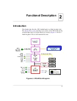
Page 33: ...am of the overall board architecture Figure 2 1 VP22 Block Diagram 33 MHz 32 bit PCI Bus EIDE B EIDE A ATA 100 LPC Bus EIA 232 Floppy IrDA 10 100 Ethernet AC97 82802BA Firmware Hub 82801BA I O Controller Hub2 ICH2 Socket 370 Processor Three 168 pin 3 3V DIMM sockets Analog Video PCI Slot PCI Slot PCI Slot PCI Slot Keyboard mouse Intel 82815E SVGA 1600 X 1200 256 colors IEEE 1284 USB A USB B EIA 23...

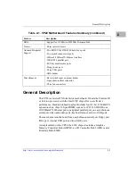
Page 34: ...or 128KB on die ATC for the Celeron processor DRAM Three 168 pin DIMM sockets 3 3V with serial presence detect SPD SDRAM PC133 at 133 MHz FSB Unbuffered non ECC no parity Supports 16 32 64 128 256MB DIMM types Intel 815E chipset Intel 82802BA Firmware Hub FWH Intel 82815 Graphics Memory Controller Hub GMCH Intel 82801BA I O Controller Hub2 ICH2 Environmental Monitoring Hardware monitor 83627HF all...

Page 35: ...e board for an asynchronous serial port floppy port IrDA port internal USB port and two EIDE ports As implemented on the VP22 the 815E chipset includes a Graphics Memory Controller Hub GMCH an I O Controller Hub2 ICH2 and a Firmware Hub FWH BIOS Support for 4 8 Mbit in 82802BA Firmware Hub Timers Three interval timers Onboard Peripheral Support Two EIDE Ultra DMA 100 hard drive ports Two asynchron...

Page 36: ... timings of the slowest DRAMs installed This motherboard supports up to 512MB of SDRAM memory with three 168 pin DIMM sockets It supports 3 3 V single or double sided DIMMs and the individual SDRAMs on the DIMMs must be x8 or x16 parts x4 parts are not supported The DIMM sockets can be populated in any order SDRAM operation at 133MHz and 100MHz is supported L2 Cache The Pentium III has an on die 2...

Page 37: ...er interface using an Intel 82562EM integrated Ethernet device The Ethernet interface is accessed via an industry standard rear panel mounted RJ 45 connector The 82562EM chip is assigned an Ethernet Station Address The address is unique for each board assembly and is displayed on a label affixed to the board In addition the Ethernet address is stored in the configuration ROM interfaced to the 8256...

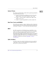
Page 38: ...f 3F8h and 2F8h respectively This default configuration also assigns COM1 to IRQ4 and COM2 to IRQ3 Peripheral Parallel Port All parallel I O interface signals are routed to an industry standard DB 25 connector accessible from the rear panel This port supports the full IEEE 1284 capability which provides the basic printer interface Firmware initializes the parallel port as LPT1 with ISA I O base ad...

Page 39: ...es of battery backed RAM is available for use by the BIOS A separate 3 V coin cell battery provides battery backup BIOS The VP22 supports the Intel 82802BA Firmware Hub FWH A boot block device allows recovery of the BIOS in the event of a catastrophic failure power fail during BIOS update Flash write protection is implemented under software control and this bit must be set to 1 before any write is...

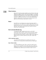
Page 40: ... board by generating the CPU PCI and IDE resets This board can also be reset by an external switch that is connected to an onboard header Environmental Monitoring The Winbond 83627HF hardware monitor device on the VP22 motherboard provides a number of useful system management features These features include temperature fan and voltage monitoring The hardware monitor allows software to monitor volt...

Page 41: ...at is listed in Appendix C Related Documentation Watchdog Timer A watchdog timer is embedded in the 83627HF hardware monitor chip The watchdog timer is an 8 bit counter with one second resolution The watchdog has either a one second granularity up to 255 seconds or a one minute granularity up to 255 minutes The watchdog output is connected to reset ...

Page 42: ......

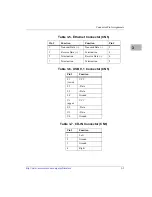
Page 43: ...onnector CN1 Pin Function Function Pin 1 Red Green 2 3 Blue VCC 4 5 Ground Ground 6 7 Ground Ground 8 9 VCC Ground 10 11 VCC 5VCDA 12 13 5HSYNC 5VSYNC 14 15 5VCLK Table 3 2 COM1 Serial Port Connector CN2 Pin Function Function Pin 1 Data Carrier Detect Receive Data 2 3 Transmit Data Data Terminal Ready 4 5 Ground Data Set Ready 6 7 Request to Send Clear to Send 8 9 Ring Indicate ...

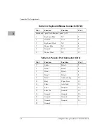
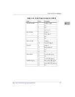
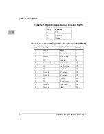
Page 44: ...nd VCC 4 5 Keyboard Clock NC 6 7 Mouse Data NC 8 9 Ground VCC 10 11 Mouse Clock NC 12 Table 3 4 Parallel Port Connector CN4 Pin Function Function Pin 1 Strobe Data 0 2 3 Data 1 Data 2 4 5 Data 3 Data 4 6 7 Data 5 Data 6 8 9 Data 7 Acknowledge 10 11 Busy Paper Error 12 13 Select Auto Feed 14 15 Error Initialize 16 17 Select In Ground 18 19 Ground Ground 20 21 Ground Ground 22 23 Ground Ground 24 25...

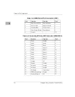
Page 45: ...tion Pin 1 Transmit Data Transmit Data 2 3 Receive Data Termination 4 5 Termination Receive Data 6 7 Termination Termination 8 Table 3 6 USB 0 1 Connector CN5 Pin Function L1 lower VCC L2 Data L3 Data L4 Ground U1 upper VCC U2 Data U3 Data U4 Ground Table 3 7 CD IN Connector CN6 Pin Function 1 Left 2 Ground 3 Ground 4 Right ...

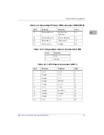
Page 46: ...inal Ready Ring Indicate 8 9 Ground 10 Table 3 9 Secondary Primary IDE Connector CN8 CN10 Pin Function Function Pin 1 Reset Ground 2 3 Data 7 Data 8 4 5 Data 6 Data 9 6 7 Data 5 Data 10 8 9 Data 4 Data 11 10 11 Data 3 Data 12 12 13 Data 2 Data 13 14 15 Data 1 Data 14 16 17 Data 0 Data 15 18 19 Ground NC 20 21 Request Ground 22 23 I O Write Ground 24 25 I O Read Ground 26 27 I O Ready Cable Select ...

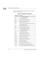
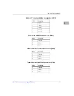
Page 47: ...ice Active Ground 40 Table 3 10 Temperature Sensor Connector CN9 Pin Function 1 VCC 2 Ground Table 3 11 ATX Power Connector CN11 Pin Function Function Pin 1 3 3 V 3 3 V 2 3 Ground 5 V 4 5 Ground 5 V 6 7 Ground PW OK 8 9 5 VSB 12 V 10 11 3 3 V 12 V 12 13 Ground PS ON_L 14 15 Ground Ground 16 17 Ground 5 V 18 19 5 V 5 V 20 Table 3 9 Secondary Primary IDE Connector CN8 CN10 Pin Function Function Pin ...

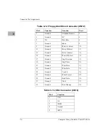
Page 48: ... Index 8 9 Ground Motor A Select 10 11 Ground Drive B Select 12 13 Ground Drive A Select 14 15 Ground Motor B Select 16 17 Ground Step Direction 18 19 Ground Step Pulse 20 21 Ground Write Data 22 23 Ground Write Gate 24 25 Ground Track 0 26 27 Ground Write Protect 28 29 Ground Read Data 30 31 Ground Side 1 32 33 Ground Disk Change 34 Table 3 13 IrDA Connector CN13 Pin Function 1 VCC 2 NC 3 IRRX 4 ...

Page 49: ...Function Chassis Speaker 1 Speaker signal 3 NC 5 NC 7 VCC 5 V Reset Button 2 Ground 4 Reset signal 6 NC 9 NC Power Switch 8 Ground 10 Power on signal Keylock 11 Ground 13 Keyboard lock 12 NC 14 NC Power LED 15 Power LED signal 17 NC 19 Power LED pull up Hard Disk LED 16 Hard Disk LED signal 18 Hard Disk LED pull up 20 NC ...

Page 50: ...3 16 Compact Floppy Disk Drive Connector CN16 Pin Function Function Pin 1 Power Index 2 3 Power Drive A Select 4 5 Power Disk Change 6 7 NC Data Rate 8 9 Extended Density Motor A Select 10 11 NC Step Direction 12 13 NC Step Pulse 14 15 Ground Write Data 16 17 Ground Write Gate 18 19 NC Track 0 20 21 NC Write Protect 22 23 Ground Read Data 24 25 Ground Side 1 26 ...

Page 51: ...l USB 2 Connector CN17 Pin Function 1 VCC 2 Data 3 Data 4 Ground 5 Ground Table 3 18 CPU Fan Connector FN1 Pin Function 1 Ground 2 Power 3 Sense Table 3 19 Chassis Fan Connector FN2 Pin Function 1 Ground 2 Power 3 Sense Table 3 20 Second Fan Connector FN3 Pin Function 1 Ground 2 Power 3 Sense ...

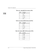
Page 52: ... Table 3 21 Audio MIC IN Connector PH1 Pin Function 1 Ground 2 MIC 3 Ground 4 Ground 5 MIC Table 3 22 Audio LINE IN Connector PH2 Pin Function 1 Ground 2 INR 3 Ground 4 Ground 5 INL Table 3 23 Audio LINE OUT Connector PH3 Pin Function 1 Ground 2 OUTR 3 Ground 4 Ground 5 OUTL ...

Page 53: ...MHz Celeron processor 0 63 A typ at 5V 3 3 A max at 5V 0 05 A typ at 5V 0 05 A max at 5V 0 12 A typ at 12V 0 12 A max at 12V 0 10 A typ at 12V 0 10 A max at 12V 1 9 A typ at 3 3V 1 9 A max at 3 3V 0 03 A typ at 5VSB 0 03 A max at 5VSB 733 MHz Pentium III processor 1 15 A typ at 5V 5 0 A max at 5V 0 05 A typ at 5V 0 05 A max at 5V 0 24 A typ at 12V 0 24 A max at 12V 0 24 A typ at 12V 0 24 A max at ...

Page 54: ...ng 5 to 95 noncondensing Vibration Operating Nonoperating 0 5 G peak from 10 to 1000 Hz random 6 0 G peak from 10 to 1000 Hz random Physical Dimensions Motherboard Width 9 6 inches 244 mm Length 9 6 inches 244 mm Motherboard Rear I O Connectors Ethernet interface One RJ 45 connector on rear panel Serial port interface asynchronous One DB 9 connector on rear panel and one 10 pin header Parallel por...

Page 55: ...nfiguration It identifies thermally significant components and lists the corresponding maximum allowable component operating temperatures It also provides example procedures for component level temperature measurements Thermally Significant Components The following table summarizes components that exhibit significant temperature rises These are the components that should be monitored in order to a...

Page 56: ...Thermally Significant Components Reference Designator Generic Description Max Allowable Component Temperature deg C Measurement Location U1 ALC200 Audio Codec 110 Case U7 82562EM Platform LAN Connect Device 135 Case U9 566MHz FC PGA Celeron Processor 733MHz FC PGA PIII Processor 866MHz FC PGA PIII Processor 90 80 80 Junction Junction Junction U10 82815 Graphics and Memory Controller Hub GMCH 116 C...

Page 57: ...owing sections outline general temperature measurement methods For the specific types of measurements required for thermal evaluation of this board see Table B 1 Preparation We recommend 40 AWG American wire gauge thermocouples for all thermal measurements Larger gauge thermocouples can wick heat away from the components and disturb air flowing past the board U9 U14 U7 U15 U10 U1 ...

Page 58: ...ture at the center of the top of the component Make sure there is good thermal contact between the thermocouple junction and the component We recommend you use a thermally conductive adhesive such as Loctite 384 If components are covered by mechanical parts such as heatsinks you will need to machine these parts to route the thermocouple wire Make sure that the thermocouple junction contacts only t...

Page 59: ...NK BOTTOM VIEW ISOMETRIC VIEW Machined groove for thermocouple wire routing Thermocouple junction bonded to component Heatsink base Thermal pad Through hole for thermocouple junction clearance may require removal of fin material Also use for alignment guidance during heatsink installation Machined groove for thermocouple wire routing ...

Page 60: ...ature by placing the thermocouple downstream of the component This method is conservative since it includes heating of the air by the component The following figure illustrates one method of mounting the thermocouple Figure B 3 Measuring Local Air Temperature Thermocouple junction PWB Tape thermocouple wire to top of component Air flow ...

Page 61: ...iterature site http www motorola com computer literature To obtain the most up to date product information in PDF or HTML format visit http www motorola com computer literature Manufacturers Documents For additional information refer to the following table for manufacturers data sheets or user s manuals As an additional help a source for the listed Table C 1 Motorola Computer Group Documents Docum...

Page 62: ... 24365815 pdf Pentium III Processor for the PGA370 socket at 500 MHz to 1 0B GHz Datasheet Intel Corporation http developer intel com design pentiumiii datashts 245264 htm 24526406 pdf Intel 815 Series Chipset 82815 Graphics and Memory Controller GMCH Datasheet Intel Corporations http developer intel com design chipsets datashts 290688 htm 29068801 pdf Intel 82801BA I O Controller Hub2 ICH2 Datash...

Page 63: ...orola Computer Group OEM Services http www motorola com computer support Intel Corporation http www intel com Table C 3 Related Specifications Document Title and Source Publication Number Peripheral Component Interconnect PCI Local Bus Specification Revision 2 0 2 1 2 2 PCI Special Interest Group http www picmg com PCI Local Bus Specification IEEE PCI Mezzanine Card Specification PMC Institute of ...

Page 64: ......

Page 65: ...loppy disk drive CN16 3 8 CPU fan FN1 3 9 Ethernet CN5 3 3 floppy disk drive CN12 3 6 front panel CN14 3 7 internal USB 2 CN17 3 9 IrDA CN13 3 6 keyboard mouse CN3 3 2 open chassis alarm CN15 3 8 parallel CN4 3 2 second fan FN3 3 9 secondary primary IDE CN8 10 3 4 SVGA CN1 3 1 temperature sensor CN9 3 5 USB0 1 CN5 3 3 controllers Intel 82562EM Ethernet 2 5 Intel 82801BA I O hub 2 2 2 8 Intel 82802...

Page 66: ... 1 14 M manual conventions xv manufacturers documents C 1 memory 2 4 motherboard installation 1 7 preparation 1 3 mouse port 2 6 N non volatile RAM NVRAM 2 7 O onboard battery replacing 1 14 open chassis alarm 2 8 operating temperatures maximum B 1 P parallel port 2 6 PCI adapter board installation 1 9 PCI slots 2 5 pin assignments 3 1 to 3 10 ATX power connector 3 5 audio LINE IN connector 3 10 a...

Page 67: ...2 relative humidity A 2 reset circuit 2 8 S SDRAM 2 4 serial ports 2 6 shielded cables 2 4 specifications board A 1 specifications related C 2 startup overview 1 2 suggestions submitting xiv T temperature measurement B 1 B 3 B 4 temperature monitor CPU 2 8 temperature range A 2 temperatures component B 1 thermal performance B 1 thermocouple mounting B 5 timers programmable 2 7 typeface meaning of ...

Reviews: