LX2
plus / advanced and LX4 plus / advanced
B2270901
Content is subject to change without notice!
42
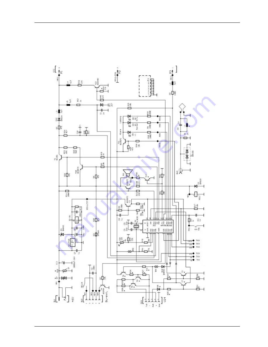
5.13
Charger Unit Schematic PCB No. 228.01.xx
Flash programming
BR1 = close after flash programming
BR2 open = relay active until reset
BR2 closed = relay active for 10s
* optional placement


