background image


miriac MPX-S32G274A User Manual 

V2.1 

47/76 


© MicroSys Electronics GmbH 2020 


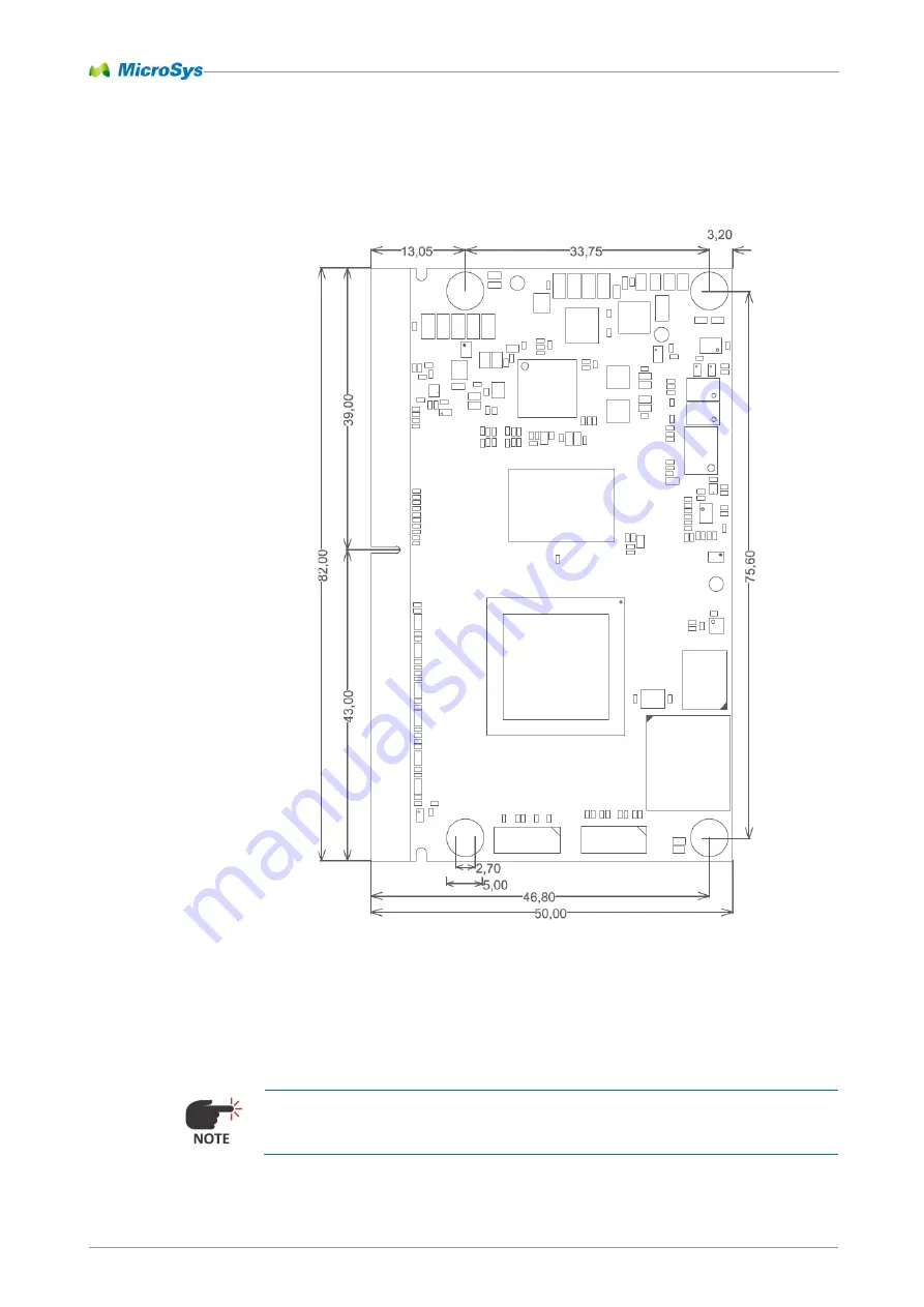
5.6 

Board Outline 

The  f ollowing drawing shows the mechanical  outline (82x50mm)  of  the 
 MPX-S32G274A  module: 


The  mounting holes require  M2.5 screws.  


For 3D data files please contact MicroSys. 


Figure 5-4 Board dimensions


Summary of Contents for miriac MPX-S32G274A

Page 1: ...miriac MPX S32G274A User Manual HW Revision 2 V2 1...

Page 2: ...11 Electronic DIP Switch 31 4 12 Interface Description 33 4 12 1 Definition of Primary Interfaces 33 4 12 2 JTAG 33 4 12 3 AURORA 33 4 12 4 ADC 33 4 12 5 CAN 34 4 12 6 RGMII 34 4 12 7 ULPI USB 35 4 12...

Page 3: ...s in this document MicroSys Electronics GmbH neither gives any guarantee nor accepts any liability whatsoever for consequential damages resulting from the use of this manual or its associated product...

Page 4: ...ent which is dependent on the preferred carrier and the location where you want to have it shipped to by sending a request to MicroSys Electronics GmbH Muehlweg 1 82054 Sauerlach Germany In your reque...

Page 5: ...ble 1 Symbols 1 5 2 Conventions Symbol Explanation xxx_B denotes a low active signal denotes the signal flow in the direction shown denotes the signal flow in the direction shown denotes the signal fl...

Page 6: ...ing operation to avoid burns and operate the unit in a well ventilated location Provide an appropriate cooling solution as required Electrostatic discharge ESD can damage the unit Always take the nece...

Page 7: ...ber of the MPX module family based on NXP s S32G274A network processor SoC MicroSys Electronics GmbH offers a Development Kit which uses the key features of the module The customer can test the operat...

Page 8: ...4GB LPDDR4 SDRAM Serial NOR flash as boot or storage device 16GB eMMC flash as boot or storage device Clock generators for SOC and interface clocks I C EEPROM I C temperature sensor I C RTC Voltage re...

Page 9: ...3 06 W 24V 3 36 W 30V 3 49 W Table 4 Typicalpower consumption at U Boot prompt 3 5 Cooling In chapter 3 4 the typical power consumption of the MPX S32G274A module was specified With this information a...

Page 10: ...escribed in chapter 4 10 and the following sections The signal names in the following two tables do not show all available options for each pin Pin multiplexing can only be implemented in combination...

Page 11: ...USB_STP T27 GND T28 RGMII2_TX_EN USB_DIR T29 RGMII2_TX_CLK USB_CLK T30 GND T31 RGMII1_MDC T32 RGMII1_MDIO T33 GND T34 RGMII1_RXD3 T35 RGMII1_RXD2 T36 RGMII1_RXD1 T37 RGMII1_RXD0 T38 GND T39 RGMII1_RX...

Page 12: ..._TXD2 T63 RGMII0_TXD1 T64 RGMII0_TXD0 T65 GND T66 RGMII0_TX_EN T67 RGMII0_TX_CLK T68 GND T69 PCIE1_RX0_N T70 PCIE1_RX0_P T71 GND T72 PCIE1_RX1_N T73 PCIE1_RX1_P T74 GND T75 PCIE0_RX0_N T76 PCIE0_RX0_P...

Page 13: ...N T97 AUR_CLK_P T98 GND T99 AUR_TX2_N T100 AUR_TX2_P T101 GND T102 AUR_TX0_N T103 AUR_TX0_P T104 GND T105 AUR_TX1_N T106 AUR_TX1_P T107 GND T108 AUR_TX3_N T109 AUR_TX3_P T110 GND T111 PB02 T112 PB07 T...

Page 14: ...ns GPIO T129 GND T130 SEL_CLK_RC EP T131 RCW_SEL T132 MUX_SEL T133 VCC_RTC T134 3V3_EXT T135 I2C_SCL_PROG T136 I2C_SDA_PROG T137 GND T138 GND T139 GND T140 GND T141 GND T142 GND T143 GND T144 GND T145...

Page 15: ...B4 ADC_CH_09 B5 ADC_CH_08 B6 GND B7 ADC_CH_07 B8 ADC_CH_06 B9 GND BK1 PMIC_STBY BK2 PMIC_VDD_OK B10 ADC_CH_05 B11 ADC_CH_04 B12 GND B13 ADC_CH_03 B14 ADC_CH_02 B15 GND B16 ADC_CH_01 B17 ADC_CH_00 B18...

Page 16: ...B39 GND B40 CAN07_RX INPUT B41 CAN07_TX B42 GND B43 CAN08_RX INPUT B44 CAN08_TX B45 GND B46 CAN09_RX INPUT B47 CAN09_TX B48 GND B49 CAN10_RX INPUT B50 CAN10_TX B51 GND B52 CAN11_RX INPUT B53 CAN11_TX...

Page 17: ...15_DSPI1_SIN B76 PA07_DSPI1_CS0 B77 GND B78 PA11_DSPI5_SOUT B79 PA09_DSPI5_SCK B80 PA10_DSPI5_SIN B81 PA12_DSPI5_CS0 B82 JTAG_TCK B83 JTAG_TDO B84 JTAG_TDI B85 JTAG_TMS B86 JCOMP B87 GND B88 PF03_CLKO...

Page 18: ...LIN2_TX B113 GND B114 LIN3_RX INPUT B115 LIN3_TX B116 GND B117 PCIE1_CLKC_N B118 PCIE1_CLKC_P B119 GND B120 PCIE0_CLKC_N B121 PCIE0_CLKC_P B122 GND B123 PMIC_FSOUT B124 PMIC_FIN B125 VDD_OTP B126 PMI...

Page 19: ...ectronicsGmbH 2020 Pin Pin Name Primary Function Alternate Functions GPIO B141 GND B142 GND B143 GND B144 GND B145 GND B146 GND B147 GND B148 VIN B149 VIN B150 VIN B151 VIN B152 VIN B153 VIN B154 VIN...

Page 20: ...t track the reference voltages and generate a copy which can carry higher loads The following diagram shows the structure of the power supplies The following table shows the internal connections Modul...

Page 21: ...ipheral devices PMIC_RST and RST are identical signals The only difference is that RST could be disconnected by a zero ohm resistor The S32G274A provides dedicated reset signals for eMMC and LPDDR4 me...

Page 22: ...with the NXP documentation they are referred to as PCIE0 and PCIE1 Each SerDes channel requires a clock which can be configured as 100MHz or 125MHz clock depending on PCIe or SGMII use J12 PI6C557 S3...

Page 23: ...nal Pin Signal I O Range Signal conditioning Frequency AB15 PCIE0_CLK_P T123 PCIE0_CLKIN_P HCSL 100 MHz AC15 PCIE0_CLK_N T122 PCIE0_CLKIN_N HCSL 100 MHz Table 10 PCIe clock for endpoint configuration...

Page 24: ...C2_SCL VREF3 PU 4k7 400 kHz AC13 CLKOUT_P T82 CLK_OUT_P VREF1 SR 0R AB13 CLKOUT_N T81 CLK_OUT_N VREF1 SR 0R AC11 AUR_CLK_P T97 AUR_CLK_P VREF1 t b d AB11 AUR_CLK_N T96 AUR_CLK_N VREF1 t b d W9 TCK B82...

Page 25: ...RCON mode is not supported by the MPX S32G274A module FUSE_SEL 0 BOOTMOD0 ball W10 BOOTMOD1 ball W11 Ethernet boot config Boot Mode 0 0 No Ethernet Serial Boot 0 1 SGMII Serial Boot 1 0 RCON 1 1 Rese...

Page 26: ...edge of the PCB Reference Colour Function LD1 Green LED ON Power up sequence of the module isfinished power is good LED OFF Power fail LD2 Red LED ON SoC Power on reset isactive LED OFF Reset is inac...

Page 27: ...ckup voltage is optional and needs to be provided from the carrier if buffering is desired The following table shows the internal connection Module Connector Pin Signal I O Range Description T133 VCC_...

Page 28: ...e Remote temperature monitoring S32G274A s temperature diode Two interrupts for adjusting two temperature thresholds Ambient 0 C 70 C Ambient 40 C 125 C Local Temperature of the sensor itself Max 1 C...

Page 29: ...IO1 J19 4 THERM_FAULT PU 10k 8 GPIO2 J21 9 RTC_IRQA PU 10k 7 GPIO3 J21 4 RTC_IRQB PU 10k 6 GPIO4 LD4 USER_LED PU 10k 5 GPIO5 HW_REV2 See Table 21 4 GPIO6 HW_REV1 3 GPIO7 HW_REV0 Table 20 GPIO Expander...

Page 30: ...boot devices are supported J4 is classified as primary EEPROM to store the boot configuration for SD card boot mode and it can also be write protected see chapter 4 11 J14 is the secondary EEPROM used...

Page 31: ...o Table 28 and provides six persistent output signals to configure the module At power up the values at MUX_OUT_x pins are either loaded from EEPROM Byte0 or MUX_IN hardware strapping inputs depending...

Page 32: ...CLK_P N 125 MHz SoC PLL PCIE0_CLKC_P N 125 MHz ST1 B120 B121 B CLKGEN2_100M 125M 1 1 PCIE1_CLK_P N 100 MHz SoC PLL PCIE1_CLKC_P N 100 MHz ST1 B117 B118 0 PCIE1_CLK_P N 125 MHz SoC PLL PCIE1_CLKC_P N 1...

Page 33: ...signals are used onboard see chapter 10 6 4 12 2 JTAG The JTAG chain of the MPX S32G274A includes the S32G274A processor only The JTAG port is directly connected to the MXM module connector The JTAG i...

Page 34: ...ured as GPIO The pins are listed in the Appendix in chapter 10 4 and 10 5 4 12 6 RGMII The S32G274A provides MACs for three RGMII interfaces each RGMII port has a dedicated MDIO interface The pins are...

Page 35: ...five I C busses which run at up to 400kHz I2C3 is not available as primary interface I2C4 is explicitly used for the power management chip on the module The pins are listed in the Appendix in chapter...

Page 36: ...29 I2C1 bus map I2C2 map Device A6 A5 A4 A3 A2 A1 A0 R W Addr Table 30 I2C2 bus map I2C 3 is available by multiplexing functions Primary interface is FlexCAN3 I2C4 map Device A6 A5 A4 A3 A2 A1 A0 R W...

Page 37: ...MT35XU512ABA1G12 Ball Signal Pin Signal I O Range G21 QSPI1_A_CS0 C2 CS 1 8V K20 QSPI1_A_SCK B2 CLK 1 8V K23 QSPI_A_DQS C3 DQS B3 E5 C1 GND L18 QSPI1_A_DATA0 D3 D0 1 8V L19 QSPI1_A_DATA1 D2 D1 1 8V L...

Page 38: ...or USB on the carrier for example The pins are listed in the Appendix in chapter 10 4 and 10 5 See chapter 4 12 12 for the LINFlexD controller which also supports UART mode 4 12 12 LIN The MPX S32G274...

Page 39: ...e is controlled by SD0_VSELECT from the SoC S32G274A Ball Signal Signal Conditioning Function G19 SD0_VSELECT PD 10k 0 3 3V 1 1 8V Table 33 SDHC voltage select VCC_SDHC_1V8 3V3 is a reference voltage...

Page 40: ...PCIe x2 100 MHz PCIe x1 SGMII 1 25 Gbps 100 MHz SGMII 1 25 Gbps SGMII 1 25 Gbps 125 MHz 100 MHz SGMII 3 125 Gbps N A 125 MHz Table 35 SerDes 1 working modes The MPX S32G274A generates four clock pair...

Page 41: ...miriac MPX S32G274A User Manual V2 1 41 76 MicroSys ElectronicsGmbH 2020 Figure 4 8 SerDes clock routing...

Page 42: ...MicroSys ElectronicsGmbH 2020 5 Mechanical Description 5 1 Edge Connector The MPX S32G274A module has 314 edge finger contacts Appropriate sockets on the carrier provide 314 pins with 0 5mm pitch and...

Page 43: ...he same 5 3 Current Numbering Scheme The differences between 310 pin and 314 pin connectors are four key pins that do not carry signals on 310 pin connectors They are physically not present These key...

Page 44: ...pins previously used as key pins see chapter 5 2 The pin layout is asymmetric so the pins are unequally distributed among top and bottom side edge fingers Side Pin Count Pin Labels Bottom 158 B1 B9 B...

Page 45: ...he module The connectors usually have deviating mechanical pads thus drop in replacements may require a combined PCB footprint Please check the manufacturers datasheets for details The recommended con...

Page 46: ...checked for bent or dirty contacts Check the module and the carrier for foreign or loose parts which do not belong to the boards The screws should have clean threads and be tightened with a maximum to...

Page 47: ...MicroSys ElectronicsGmbH 2020 5 6 Board Outline The following drawing shows the mechanical outline 82x50mm of the MPX S32G274A module The mounting holes require M2 5 screws For 3D data files please co...

Page 48: ...40 mm DIM C Carrier partsunder the module DIM D minus DIM B DIM D Board to board height Depends on connectortype DIM E Connectorproduct height Depends on connectortype Table 39 Construction height ove...

Page 49: ...miriac MPX S32G274A User Manual V2 1 49 76 MicroSys ElectronicsGmbH 2020 5 9 Component Layout Top Side Figure 5 6 Top Components...

Page 50: ...erence Type Function ST1 Edge Connector Connection to carrier J1 S32G274A SoC J2 PMIC Regulator powermanagement J3 LPDDR4 Memory J4 Primary Serial RCON EEPROM J6 eMMC Memory J8 ElectronicDIP switch J1...

Page 51: ...miriac MPX S32G274A User Manual V2 1 51 76 MicroSys ElectronicsGmbH 2020 5 10 Component Layout Bottom Side Figure 5 7 Bottom components...

Page 52: ...l V2 1 52 76 MicroSys ElectronicsGmbH 2020 Part Reference Type Function J12 PI6C557 Clock Generator J16 PI6C557 Clock Generator J21 PCF85263ATL RTC LD1 LD2 LD3 LD4 Side Looker LED Reset Power User LED...

Page 53: ...or the SD card if that interface is implemented on the carrier The standard MicroSys carrier CRX S32G has an SD card interface Basically the bootloader carries out the following tasks Pin configuratio...

Page 54: ...als Provide an EMI proof housing for final system 7 2 ESD For technical reasons there is no ESD protection on the MPX S32G274A Please provide sufficient protection on the carrier and or system level 7...

Page 55: ...mbH 2020 7 4 Climatic conditions The relative humidity during operation or storage of the module may not exceed 10 to 90 non condensing 7 5 RoHS All components on the MPX S32G274A are RoHS compliant a...

Page 56: ...s responsibility to make sure all errata published by the manufacturer of each component are taken note of The manufacturer s advice should be followed If desired MicroSys Electronics GmbH can suppor...

Page 57: ...0 05 18 1 2 310 pin JAE obsolete added alternatives 2020 11 11 2 0 Hardware Revision 2 InitialRelease Version Changed input supplyrange Added TK1 TK2 BK1 BK2 pins on formerKEY pins Renamed MACx pinsto...

Page 58: ...C Inter Integrated Circuit JTAG Joint Test Action Group LED LightEmitting Diode LIN Local InterconnectNetwork LPDDR Low Power Double Data Rate memory MCU Microcontroller Unit PD Pull Down Resistor PU...

Page 59: ...2 Figure 4 4 LEDs 26 Figure 4 5 Temperature sensor accuracy 28 Figure 4 6 Electronic DIP Switch Structure 31 Figure 4 7 SDHC routing 39 Figure 4 8 SerDes clock routing 41 Figure 5 3 MXM Connector pin...

Page 60: ...tage 27 Table 18 RTC IRQs 27 Table 19 Temperature sensor IRQs 28 Table 20 GPIO Expander Pin description 29 Table 21 GPIO Expander Hardware Revision 29 Table 22 GPIO Expander IRQ 29 Table 23 Boot confi...

Page 61: ...VCC_SDHC_1V8 3V3 22R T5 GND GND T6 SD_D0 G22 PD01 SDHC INOUT VCC_SDHC_1V8 3V3 0R T7 SD_D1 E20 PD02 SDHC INOUT VCC_SDHC_1V8 3V3 0R T8 SD_D2 H19 PD03 SDHC INOUT VCC_SDHC_1V8 3V3 0R T9 SD_D3 H20 PD04 SD...

Page 62: ...LPI OUT INOUT VREF1 1V8 10R T25 RGMII2_TXD1 USB_NXT N22 PL11 RGMII ULPI OUT IN VREF1 1V8 10R T26 RGMII2_TXD0 USB_STP P22 PL10 RGMII ULPI OUT OUT VREF1 1V8 10R T27 GND GND T28 RGMII2_TX_EN USB_DIR L23...

Page 63: ...PE15 RGMII INOUT VREF1 1V8 PU 10k 0R T52 GND GND T53 RGMII0_RXD3 W22 PH09 RGMII IN VREF1 1V8 10R T54 RGMII0_RXD2 W21 PH08 RGMII IN VREF1 1V8 10R T55 RGMII0_RXD1 Y23 PH07 RGMII IN VREF1 1V8 10R T56 RG...

Page 64: ...T77 GND GND T78 PCIE0_RX1_N AC18 SERDES IN VREF1 1V8 T79 PCIE0_RX1_P AB18 SERDES IN VREF1 1V8 T80 GND GND T81 CLK_OUT_N AB13 CLOCK OUT VREF1 1V8 0R T82 CLK_OUT_P AC13 CLOCK OUT VREF1 1V8 0R T83 GND GN...

Page 65: ...1 1V8 T103 AUR_TX0_P AC8 AURORA OUT VREF1 1V8 T104 GND GND T105 AUR_TX1_N AC6 AURORA OUT VREF1 1V8 T106 AUR_TX1_P AB6 AURORA OUT VREF1 1V8 T107 GND GND T108 AUR_TX3_N AC5 AURORA OUT VREF1 1V8 T109 AUR...

Page 66: ...TRL IN VREF4 3V3 PU 4k7 100R T128 RST J2 19 CTRL OUT VREF4 3V3 PU 2k2 T129 GND GND T130 SEL_CLK_RC EP TR9 1 CTRL IN VREF4 3V3 PU 10k T131 RCW_SEL TR3 1 J14 2 J14 3 CTRL IN 3V3_EXT PU 4k7 T132 MUX_SEL...

Page 67: ...icroSys ElectronicsGmbH 2020 T143 GND GND T144 GND GND T145 GND GND T146 VIN POWER 9 30V T147 VIN POWER 9 30V T148 VIN POWER 9 30V T149 VIN POWER 9 30V T150 VIN POWER 9 30V T151 VIN POWER 9 30V T152 V...

Page 68: ...REF1 1V8 B2 ADC_CH_10 A20 ADC IN VREF1 1V8 B3 GND GND B4 ADC_CH_09 B20 ADC IN VREF1 1V8 B5 ADC_CH_08 A19 ADC IN VREF1 1V8 B6 GND GND B7 ADC_CH_07 C22 ADC IN VREF1 1V8 B8 ADC_CH_06 D23 ADC IN VREF1 1V8...

Page 69: ...GND GND B25 CAN02_RX C15 PJ04 CAN IN VREF4 3V3 B26 CAN02_TX D10 PJ03 CAN OUT VREF3 3V3 B27 GND GND B28 CAN03_RX D15 PJ06 CAN IN VREF4 3V3 B29 CAN03_TX C11 PJ05 CAN OUT VREF3 3V3 B30 GND GND B31 CAN04_...

Page 70: ...PK03 CAN OUT VREF3 3V3 B51 GND GND B52 CAN11_RX B15 PK06 CAN IN VREF4 3V3 B53 CAN11_TX D11 PK05 CAN OUT VREF3 3V3 B54 GND GND B55 CAN12_RX F13 PK08 CAN IN VREF4 3V3 B56 CAN12_TX C10 PK07 CAN OUT VREF3...

Page 71: ...F3 3V3 B77 GND GND B78 PA11_DSPI5_SOUT D8 PA11 SPI OUT VREF3 3V3 B79 PA09_DSPI5_SCK B8 PA09 SPI OUT VREF3 3V3 B80 PA10_DSPI5_SIN E13 PA10 SPI IN VREF4 3V3 B81 PA12_DSPI5_CS0 C7 PA12 SPI IN VREF3 3V3 B...

Page 72: ...B14 CAN IN VREF3 3V3 B103 PB13_FXCAN3_TX G7 PB13 CAN OUT VREF3 3V3 B104 GND GND B105 LIN0_RX A12 PL00 LIN IN VREF4 3V3 B106 LIN0_TX F10 PK15 LIN OUT VREF3 3V3 B107 GND GND B108 LIN1_RX C13 PC04 LIN IN...

Page 73: ...PU 5k11 B127 PMIC_PSYNC J2 29 CTRL IN VREF4 3V3 PD 0R B128 PMIC_FOUT AMUX J2 24 CTRL OUT VREF4 3V3 B129 GND GND B130 PC09_UART0_TX U11 PC09 UART OUT VREF3 3V3 B131 PC10_UART0_RX Y12 PC10 UART IN VREF3...

Page 74: ...icroSys ElectronicsGmbH 2020 B145 GND GND B146 GND GND B147 GND GND B148 VIN Power 9 30V B149 VIN Power 9 30V B150 VIN Power 9 30V B151 VIN Power 9 30V B152 VIN Power 9 30V B153 VIN Power 9 30V B154 V...

Page 75: ...MC cannot be used PD01 SDC eMMC GPIO possible in case SEL_EMMC_SDHC is always low eMMC cannot be used PD02 SDC eMMC GPIO possible in case SEL_EMMC_SDHC is always low eMMC cannot be used PD03 SDC eMMC...

Page 76: ...F10 QSPI N A PF11 QSPI N A PF12 QSPI N A PF13 QSPI N A PF14 QSPI N A PA02 PA02_BOOTMOD1 CONFIG N A PA03 PA03_BOOTMOD2 CONFIG N A PB00 PB00_I2C0_SDA I2C N A PB01 PB01_I2C0_SCL I2C N A PC01 PC01_I2C4_SD...

Reviews: