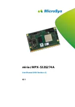
miriac MPX-S32G274A User Manual
V2.1
10/76
© MicroSys Electronics GmbH 2020
4
Technical Description
4.1
Pinouts
The signal direction is from the module’s view. For example,
PCIE0_TX0_N, pin T90, is
an output from the module and an input to peripheral devices on the carrier.
The f ollowing table gives an overview of the 314
pins of the module’s edge finger.
For a detailed connector description see chapter 5.1. The pins will be described in
chapter 4.10 and the f ollowing sections.
The signal names in the f ollowing two tables do not show all available options f or
each pin. Pin multiplexing can only be implemented in combination with the
vendor’s datasheet.
4.1.1
Module Connector
– Top Pins
Pin
Pin Name /
Primary Function
Alternate
Functions
GPIO?
T1
GND
---
---
T2
SD_CLK
---
T3
GND
---
---
T4
SD_CMD
---
T5
GND
---
---
T6
SD_D0
---
T7
SD_D1
---
T8
SD_D2
---
T9
SD_D3
---
TK1
VCC_SDHC_1V8/3V3
---
---
TK2
PMIC_FCCU1_OUT
---
---
T10
GND
---
---
T11
GND
---
---
T12
RGMII2_MDC/DSPI0_CS7
T13
RGMII2_MDIO
T14
GND
---
---
T15
RGMII2_RXD3/USB_D7
T16
RGMII2_RXD2/USB_D6
T17
RGMII2_RXD1/USB_D5
T18
RGMII2_RXD0/USB_D4
T19
GND
---
---
T20
RGMII2_RXDV/USB_D3


