Summary of Contents for IGLOO nano Starter Kit

Page 1: ...IGLOO nano Starter Kit User s Guide ...

Page 2: ...ration of Board Components 19 Clock Oscillator 19 Reset 20 Flash Freeze Switch 21 Push Button Switches 22 DIP Switches 23 User LEDs 24 I O Test Pins 24 USB to UART Interface 26 Low Cost Programming Stick LCPS 27 4 Programming 29 5 Board Demonstration 31 Powering Up the Board and Running the Demo 31 A Resources 33 B List Of Changes 35 C Product Support 37 Customer Service 37 Customer Technical Supp...

Page 3: ...w includes power driven layout PDL which can reduce the power consumption of designs up to 30 percent Since IGLOO nano devices are footprint compatible with ProASIC 3 nano devices this kit can also be used to prototype designs for ProASIC3 nano FPGAs Key Features Powered by USB cable or by external power not supplied Test points for measuring current consumption of the AGLN250V2 VQG100 USB to UART...

Page 4: ...ds on the board for debug purposes Kit Contents Table 1 lists the contents of the IGLOO nano Starter Kit Web Based Resources Listed below are the documents currently published on the Microsemi SoC Products Group website Additional documents and design examples may be added to the website in the future Users Guides and Tutorials IGLOO nano Starter Kit User s Guide www microsemi com soc documents IG...

Page 5: ...log_Libero84sp2_revA zip IGLOO Icicle VHDL Design Files www microsemi com soc documents IGLOO_Icicle_tutorial_VHDL_Libero84sp2_revA zip Board References IGLOO nano Starter Kit Board Allegro PCB file www microsemi com soc documents IGLOO_nano_StarterKit_PCB zip IGLOO nano Starter Kit Board OrCAD Schematics DSN www microsemi com soc documents IGLOO_nano_StarterKit_DSN zip IGLOO nano Starter Kit Boar...

Page 6: ......

Page 7: ...omponents and Settings This chapter describes the components and settings for the IGLOO nano Evaluation Board Block Diagram The IGLOO nano board Evaluation Board is shown in Figure 1 1 Figure 1 1 IGLOO nano Evaluation Board ...

Page 8: ...d Settings 8 Revision 3 IGLOO nano Board Stackup The IGLOO nano board is built on a four layer printed circuit board PCB 1 Top Signal Figure 1 2 2 Power 3 GND 4 Bottom Signal Figure 1 3 on page 9 Figure 1 2 Top Silkscreen ...

Page 9: ...IGLOO nano Starter Kit Revision 3 9 Figure 1 3 Bottom Silkscreen ...

Page 10: ...or VCC B1 Bank 1 Pin 1 2 selects 3 3 V Pin 3 4 selects 2 5 V Pin 5 6 selects VCC_CORE JP9 Pin 2 3 Current measurement header for JTAG supply JP10 Pin 2 3 Current measurement header for VCC FPGA core supply JP11 Pin 1 2 Voltage selection for VCC JTAG JTAG supply Pin 1 2 selects 3 3 V Pin 3 4 selects 2 5V Pin 5 6 selects VCC_CORE JP12 Pin 2 3 Current measurement header for VCC_PUMP FPGA charge pump ...

Page 11: ...e Enhanced commercial temperature Reprogrammable flash technology 1 2 V to 1 5 V single voltage operation Enhanced I O features Selectable Schmitt trigger Inputs Clock conditioning circuits CCCs and integrated PLLs Embedded SRAM and nonvolatile memory NVM In system programming ISP and security For further information refer to the IGLOO nano datasheet www microsemi com soc documents IGLOO_nano_DS p...

Page 12: ...t_n 5 agl_clk 5 IO43RSB2 33 IO44RSB2 32 IO45RSB2 31 IO46RSB2 30 IO47RSB2 29 GEC2 IO48RSB2 28 FF GEB2 IO49RSB2 27 GEA2 IO50RSB2 26 GDA2 IO34RSB2 45 GDB2 IO35RSB2 44 GDC2 IO36RSB2 43 IO37RSB2 42 IO38RSB2 41 IO39RSB2 40 IO40RSB2 36 IO41RSB2 35 IO42RSB2 34 IO BANK2 U5C AGLN250V2 VQG100 IO BANK2 U5C AGLN250V2 VQG100 GCA0 IO28RSB1 63 GCA1 IO27RSB1 62 GCB2 IO29RSB1 61 IO30RSB1 60 GDC1 IO31RSB1 59 GDC0 IO...

Page 13: ...P 52 VJTAG 56 GND1 1 GND2 9 GND3 38 GND4 51 GND5 67 GND6 88 GNDQ1 25 GNDQ2 46 GNDQ3 75 GNDQ4 99 VCOMPLF 12 VCC1 17 VCC2 37 VCC3 68 VCC4 89 VCCIB0 87 VMV0 100 VCCIB1 66 VMV1 74 VCCIB2 39 VMV2 50 VCCIB3 18 VMV3 24 VCCPLF 14 SUPPLY U5F AGLN250V2 VQG100 SUPPLY U5F AGLN250V2 VQG100 C18 10u TantA C18 10u TantA VCC_B0 VCC_B1 VCC_B2 VCC_B3 VCC VCC_PLF VCC_PUMP VCC_JTAG FPGA Decoupling Capacitors Place clo...

Page 14: ......

Page 15: ... the current ratings for each voltage rail Figure 2 1 shows the schematic for the power LED9 Power Modes In addition to the board the IGLOO nano FPGA offers power advantages Some key power advantages of the IGLOO nano FPGAs are as follows Flash Freeze technology enables easy entry and exit from the static low power mode whereas IGLOO consumes as little as 5 µW while retaining the contents of the s...

Page 16: ... external batteries Table 2 2 Power Modes Mode VCC VCCI Core Clocks ULSICC Macro To Enter Mode To Resume Operation Trigger Active On On On On N A Initiate clock None Static Idle On On On Off N A Stop clock Initiate clock External Flash Freeze Type 1 On On On On N A Assert FF pin Deassert FF pin External Flash Freeze Type 2 On On On On Used to enter Flash Freeze mode Assert FF pin and LSICC Deasser...

Page 17: ...ring through 3 3 V or 2 5 V Once the IGLOO nano evaluation board is powered up you can evaluate power consumption using the current measurement 4 pin headers on the board Figure 2 3 Current measurement can be made without powering down the board Set the multimeter to measure current and attach the probes to pins 1 and 4 when the board is in normal operation Remove jumper from pins 2 3 for current ...

Page 18: ... 5 6 VCC_CORE 1 5V 1 2V Note Short Pins 1 2 3 3V Short Pins 3 4 2 5V Short Pins 5 6 VCC_CORE 1 5V 1 2V Note Short Pins 1 2 3 3V Short Pins 3 4 2 5V Short Pins 5 6 VCC_CORE 1 5V 1 2V 1 2 3 4 5 6 JP5 3x2 Header M JP5 3x2 Header M 1 2 3 4 5 6 JP11 3x2 Header M JP11 3x2 Header M 1 2 3 4 JP3 4x1 Header M JP3 4x1 Header M 1 2 3 4 5 6 JP8 3x2 Header M JP8 3x2 Header M 1 2 3 4 JP4 4x1 Header M JP4 4x1 Hea...

Page 19: ... devkits_boards igloonano_starter aspx Schematic Figure 3 1 shows the schematic for the clock oscillator Table 3 1 Clock Specifications Feature Specification Frequency 20 MHz Package Case SMD 3 2 mm x 2 5 mm Supply Voltage 3 3 V Current Supply 5 mA Operating Temperature 20 C to 70 C Frequency Stability 100 ppm RoHS Status RoHS compliant Duty CMOS level 1 2 VDD 40 60 Rise and Fall Time 0 2 VDD and ...

Page 20: ... in the active state for approximately 150 ms to allow the power supply and processor to stabilize Reference Additional information on this push button reset switch is available at the IGLOO nano Starter Kit website www microsemi com soc products hardware devkits_boards igloonano_starter aspx Schematic Figure 3 2 shows the schematic for reset Figure 3 2 Reset Schematic VCC_3_3 VCC_3_3 agl_reset_n ...

Page 21: ...ze technology Setting the F F switch to FF_ON will enable the Flash Freeze mode of the IGLOO nano device In the Flash Freeze schematic shown in Figure 3 4 the Schmitt device is use to reduce noise on the F F input of the IGLOO nano FPGA This Schmitt device can be bypassed with a resistor because an AGLN250 FPGA supports additional I O advanced features such as Schmitt trigger Figure 3 3 Flash Free...

Page 22: ... Schematic Figure 3 6 Jumper Header Schematic for Push Button Switches pb_sw1 pb_sw2 pb_sw3 pb_sw4 VCC_3_3 1 4 2 3 SW2 SW PUSHBUTTON SPST 2 SW2 SW PUSHBUTTON SPST 2 1 4 2 3 SW3 SW PUSHBUTTON SPST 2 SW3 SW PUSHBUTTON SPST 2 1 4 2 3 SW4 SW PUSHBUTTON SPST 2 SW4 SW PUSHBUTTON SPST 2 1 2 3 4 5 6 7 8 RP2 10K 0603x4 RPack RP2 10K 0603x4 RPack 1 4 2 3 SW1 SW PUSHBUTTON SPST 2 SW1 SW PUSHBUTTON SPST 2 pb_...

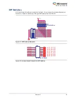
Page 23: ...ches dip_sw1 dip_sw2 dip_sw3 dip_sw4 dip_sw5 dip_sw6 dip_sw7 dip_sw8 VCC_3_3 1 2 3 4 5 6 7 8 16 15 14 13 12 11 10 9 SW5 SMD SW DIP 8 SW5 SMD SW DIP 8 1 2 3 4 5 6 7 8 9 10 11 12 13 14 15 16 RP1 10K 0603x8 RPack RP1 10K 0603x8 RPack dip_sw1 dip_sw2 dip_sw4 dip_sw3 dip_sw7 dip_sw6 dip_sw5 dip_sw8 agl_b2_p26 4 8 agl_b2_p28 4 8 agl_b2_p29 4 8 agl_b2_p30 4 8 agl_b2_p31 4 8 agl_b2_p32 4 8 agl_b2_p33 4 8 ...

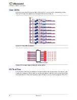
Page 24: ... 2 LED2 RED SMD LED 1206 LED2 RED SMD LED 1206 R31 470R 0603 R31 470R 0603 1 2 LED5 GREEN SMD LED 1206 LED5 GREEN SMD LED 1206 1 2 LED1 RED SMD LED 1206 LED1 RED SMD LED 1206 R34 470R 0603 R34 470R 0603 1 2 LED6 GREEN SMD LED 1206 LED6 GREEN SMD LED 1206 1 2 LED3 RED SMD LED 1206 LED3 RED SMD LED 1206 R35 470R 0603 R35 470R 0603 R32 470R 0603 R32 470R 0603 1 2 LED7 GREEN SMD LED 1206 LED7 GREEN SM...

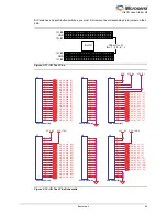
Page 25: ...8 4 6 agl_b3_p2 4 agl_b3_p3 4 agl_b3_p4 4 agl_b3_p5 4 agl_b3_p6 4 agl_b3_p7 4 agl_b3_p8 4 agl_b3_p11 4 agl_b3_p13 4 agl_b3_p20 4 6 agl_b3_p21 4 6 agl_b3_p22 4 6 agl_b3_p23 4 6 agl_b0_p95 4 agl_b0_p96 4 agl_b0_p93 4 agl_b0_p91 4 agl_b0_p92 4 agl_b0_p94 4 agl_b0_p86 4 agl_b0_p90 4 agl_b0_p84 4 agl_b0_p83 4 agl_b0_p82 4 agl_b0_p80 4 agl_b0_p79 4 agl_b0_p78 4 agl_b0_p81 4 agl_b0_p76 4 agl_b0_p77 4 agl...

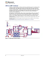
Page 26: ...soc products hardware devkits_boards igloonano_starter aspx Figure 3 13 USB to UART Interface Schematic VCC_vbus_f VCC_vbus VCC_3_3_1 VCC_usb_vbus GND_SHLD1 VCC_3_3_1 VCC_vbus GND_SHLD1 VCC_vbus agl_txd 4 agl_rxd 4 USB Connected USB in rush Limiter Ferrite Bead R48 10K 0603 R48 10K 0603 SP14 DCD SP14 DCD R41 2K7 0603 R41 2K7 0603 R38 560R 0603 R38 560R 0603 SP10 DTR SP10 DTR 1 2 3 4 5 6 U9 USBLC6 ...

Page 27: ...ramming is taking place and returns to a low level when programming has completed The IGLOO nano board uses this signal to effect a change in the value of VCC from 1 2 V to 1 5 V which is required for programming all IGLOO nano devices You do not need to have the LCPS connected to the IGLOO nano board to operate it once the FPGA has been programmed The IGLOO nano board only needs the LCPS connecte...

Page 28: ......

Page 29: ...ase format pdb or STAPL format stp to be downloaded via the FlashPro software to the IGLOO nano device fitted to the board 3 A separate USB connection is required for the IGLOO nano Board if no other power source is attached to the IGLOO nano Board 4 When using the FlashPro software select the FlashPro3 programmer The LCPS is functionally equivalent to a FlashPro programmer but designed specifical...

Page 30: ......

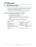
Page 31: ...a powered PC 3 Plug the USB cable into the board to power it up The board is powered from the USB connection and no external supply is required A 5 V wall jack connector is only provided on the board as an alternative if USB power is not available 4 On power up there should not be any activity on the LED reset condition 5 Refer to the table below for LEDs push button switch and DIP switch function...

Page 32: ......

Page 33: ...OO nano Overview www microsemi com soc products igloonano default aspx IGLOO nano Datasheet www microsemi com soc documents IGLOO_nano_DS pdf IGLOO nano FPGA Fabric User s Guide www microsemi com soc documents IGLOO_nano_UG pdf Microsemi FPGA and SoC Development Software www microsemi com soc products software libero default aspx ...

Page 34: ......

Page 35: ...00 part was replaced with AGLN250V2 VQG100 throughout the document References to nano Z parts were removed SAR 27593 3 11 others The FPGA Description AGLN250V2 VQG100 section was revised to change PLLs to integrated PLLs The FlashROM bits value in Table 1 2 Features of AGLN250V2 VQG100 was changed from 1 000 to 1 024 SAR 27593 11 The following figures were replaced SAR 27593 Figure 1 4 AGLN250V2 V...

Page 36: ......

Page 37: ...sues and various FAQs So before you contact us please visit our online resources It is very likely we have already answered your questions Technical Support Visit the Customer Support website www microsemi com soc support search default aspx for more information and support Many answers available on the searchable web resource include diagrams illustrations and links to other resources on the webs...

Page 38: ...ational Traffic in Arms Regulations ITAR contact us via soc_tech_itar microsemi com Alternatively within My Cases select Yes in the ITAR drop down list For a complete list of ITAR regulated Microsemi FPGAs visit the ITAR web page Regulatory and Compliance Information EU Declaration of Conformity This product complies to Directive 2011 65 EU of the European Parliament and of the Council of 8 June 2...

Page 39: ...t pins 24 IGLOO nano Evaluation Board 7 J jumpers settings 10 L LCPS 4 27 interface 27 programming 29 LEDs 24 low cost programming stick LCPS 4 27 M Microsemi SoC Products Group email 37 web based technical support 37 website 37 P product support customer service 37 email 37 My Cases 38 outside the U S 38 technical support 37 website 37 programming 29 push button reset 20 push button switches 22 R...

Page 40: ...Index 40 Revision 3 T tech support ITAR 38 My Cases 38 outside the U S 38 technical support 37 U USB to UART interface 4 User LEDs 24 W web based technical support 37 ...

Page 41: ......
Page 42: ...solutions for aerospace defense and security enterprise and communications and industrial and alternative energy markets Products include high performance high reliability analog and RF devices mixed signal and RF integrated circuits customizable SoCs FPGAs and complete subsystems Microsemi is headquartered in Aliso Viejo Calif Learn more at www microsemi com Microsemi Corporate Headquarters One E...

Reviews: