


PIC16F87XA
DS39582B-page 36
2003 Microchip Technology Inc.
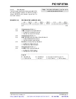
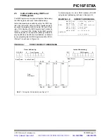
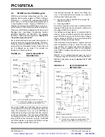
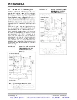
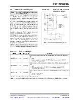
3.5
Reading Flash Program Memory
To read a program memory location, the user must write
two bytes of the address to the EEADR and EEADRH
registers, set the EEPGD control bit (EECON1<7>) and
then set control bit RD (EECON1<0>). Once the read
control bit is set, the program memory Flash controller
will use the next two instruction cycles to read the data.
This causes these two instructions immediately follow-
ing the “
BSF EECON1,RD
” instruction to be ignored.
The data is available in the very next cycle in the
EEDATA and EEDATH registers; therefore, it can be
read as two bytes in the following instructions. EEDATA
and EEDATH registers will hold this value until another
read or until it is written to by the user (during a write
operation).
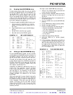
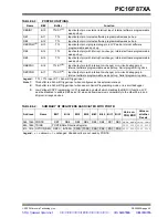
EXAMPLE 3-3:
FLASH PROGRAM READ
BSF STATUS, RP1 ;
BCF STATUS, RP0 ; Bank 2
MOVLW MS_PROG_EE_ADDR ;
MOVWF EEADRH ; MS Byte of Program Address to read
MOVLW LS_PROG_EE_ADDR ;
MOVWF EEADR ; LS Byte of Program Address to read
BSF STATUS, RP0 ; Bank 3
BSF EECON1, EEPGD ; Point to PROGRAM memory
BSF EECON1, RD ; EE Read
;
NOP
NOP ; Any instructions here are ignored as program
; memory is read in second cycle after BSF EECON1,RD
;
BCF STATUS, RP0 ; Bank 2
MOVF EEDATA, W ; W = LS Byte of Program EEDATA
MOVWF DATAL ;
MOVF EEDATH, W ; W = MS Byte of Program EEDATA
MOVWF DATAH ;
Re
q
u
ir
e
d
S
equ
en
ce
http://www.xinpian.net
提供单片机解密、IC解密、芯片解密业务
010-62245566 13810019655


