


2003 Microchip Technology Inc.
DS39582B-page 131
PIC16F87XA
11.2
Selecting the A/D Conversion
Clock
The A/D conversion time per bit is defined as T
AD
. The
A/D conversion requires a minimum 12 T
AD
per 10-bit
conversion. The source of the A/D conversion clock is
software selected. The seven possible options for T
AD
are:
• 2 T
OSC
• 4 T
OSC
• 8 T
OSC
• 16 T
OSC
• 32 T
OSC
• 64 T
OSC
• Internal A/D module RC oscillator (2-6
µ
s)
For correct A/D conversions, the A/D conversion clock
(T
AD
) must be selected to ensure a minimum T
AD
time
of 1.6
µ
s.
Table 11-1 shows the resultant T
AD
times derived from
the device operating frequencies and the A/D clock
source selected.
11.3
Configuring Analog Port Pins
The ADCON1 and TRIS registers control the operation
of the A/D port pins. The port pins that are desired as
analog inputs must have their corresponding TRIS bits
set (input). If the TRIS bit is cleared (output), the digital
output level (V
OH
or V
OL
) will be converted.
The A/D operation is independent of the state of the
CHS2:CHS0 bits and the TRIS bits.
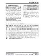
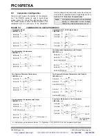
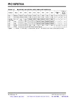
TABLE 11-1:
T
AD
vs. MAXIMUM DEVICE OPERATING FREQUENCIES (STANDARD DEVICES (F))
Note 1: When reading the port register, any pin
configured as an analog input channel will
read as cleared (a low level). Pins config-
ured as digital inputs will convert an analog
input. Analog levels on a digitally config-
ured input will not affect the conversion
accuracy.
2: Analog levels on any pin that is defined as
a digital input (including the AN7:AN0
pins) may cause the input buffer to con-
sume current that is out of the device
specifications.
AD Clock Source (T
AD
)
Maximum Device Frequency
Operation
ADCS2:ADCS1:ADCS0
2 T
OSC
000
1.25 MHz
4 T
OSC
100
2.5 MHz
8 T
OSC
001
5 MHz
16 T
OSC
101
10 MHz
32 T
OSC
010
20 MHz
64 T
OSC
110
20 MHz
RC
(1, 2, 3)
x11
(Note 1)
Note 1:
The RC source has a typical T
AD
time of 4
µ
s but can vary between 2-6
µ
s.
2:
When the device frequencies are greater than 1 MHz, the RC A/D conversion clock source is only
recommended for Sleep operation.
3:
For extended voltage devices (LF), please refer to Section 17.0 “Electrical Characteristics”.
http://www.xinpian.net
提供单片机解密、IC解密、芯片解密业务
010-62245566 13810019655


