


PIC16F716
DS41206A-page 50
Preliminary
2003 Microchip Technology Inc.
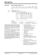
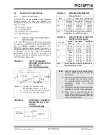
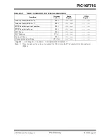
REGISTER 8-2:
ADCON1 REGISTER (ADDRESS: 9Fh)
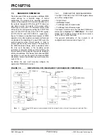
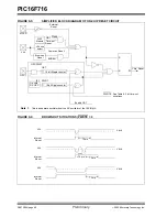
The ADRES register contains the result of the A/D
conversion. When the A/D conversion is complete, the
result is loaded into the ADRES register, the GO/DONE
bit (ADCON0<2>) is cleared and the A/D interrupt flag
bit ADIF is set. The block diagram of the A/D module is
shown in Figure 8-1.
The value that is in the ADRES register is not modified
for any Reset. The ADRES register will contain
unknown data after a Power-on Reset.
After the A/D module has been configured as desired,
the selected channel must be acquired before the
conversion is started. The analog input channels must
have their corresponding TRIS bits selected as an
input. To determine acquisition time, see Section 8.1
“A/D Acquisition Requirements”. After this
acquisition time has elapsed, the A/D conversion can
be started. The following steps should be followed for
doing an A/D conversion:
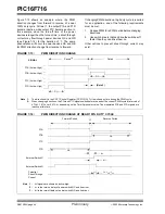
1.
Configure the A/D module:
- Configure analog pins/voltage reference/
and digital I/O (ADCON1)
- Select A/D input channel (ADCON0)
- Select A/D conversion clock (ADCON0)
- Turn on A/D module (ADCON0)
2.
Configure A/D interrupt (if desired):
- Clear ADIF bit
- Set ADIE bit
- Set GIE bit
3.
Wait the required acquisition time.
4.
Start conversion:
- Set GO/DONE bit (ADCON0)
5.
Wait for A/D conversion to complete, by either:
- Polling for the GO/DONE bit to be cleared
OR
- Waiting for the A/D interrupt
6.
Read A/D Result register (ADRES), clear bit
ADIF if required.
7.
For the next conversion, go to step 1 or step 2
as required. The A/D conversion time per bit is
defined as T
AD
. A minimum wait of 2T
AD
is
required before next acquisition starts.
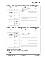
U-0
U-0
U-0
U-0
U-0
R/W-0
R/W-0
R/W-0
—
—
—
—
—
PCFG2
PCFG1
PCFG0
bit 7
bit 0
bit 7-3
Unimplemented: Read as '
0
'
bit 2-0
PCFG2:PCFG0: A/D Port Configuration Control bits
Legend:
R = Readable bit
W = Writable bit
U = Unimplemented bit, read as ‘
0
’
-n = Value at POR
‘1’ = Bit is set
‘0’ = Bit is cleared
x = Bit is unknown
PCFG2:PCFG0
AN3
RA3
AN2
RA2
AN2
RA1
AN0
RA0
V
REF
0x0
A
A
A
A
V
DD
0x1
V
REF
A
A
A
RA3
100
A
D
A
A
V
DD
101
V
REF
D
A
A
RA3
11x
D
D
D
D
V
DD
Legend:
A = Analog input, D = Digital I/O
Summary of Contents for PIC16F716
Page 6: ...PIC16F716 DS41206A page 4 Preliminary 2003 Microchip Technology Inc NOTES...
Page 35: ......
Page 56: ......
Page 60: ......
Page 88: ......
Page 92: ...PIC16F716 DS41206A page 90 Preliminary 2003 Microchip Technology Inc NOTES...
Page 108: ...PIC16F716 DS41206A page 106 Preliminary 2003 Microchip Technology Inc NOTES...
Page 110: ...PIC16F716 DS41206A page 108 Preliminary 2003 Microchip Technology Inc NOTES...
Page 124: ...PIC16F716 DS41206A page 122 Preliminary 2003 Microchip Technology Inc NOTES...


