


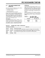


PIC16C63A/65B/73B/74B
DS30605C-page 40
2000 Microchip Technology Inc.
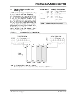
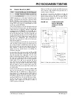
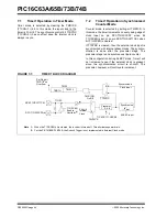
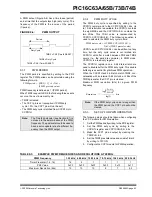
6.2
Using Timer0 with an External
Clock
The synchronization of T0CKI with the internal phase
clocks is accomplished by sampling the synchronized
input on the Q2 and Q4 cycles of the internal phase
clocks. Therefore, it is necessary for T0CKI to be high
for at least 2 T
OSC
(and a small RC delay of 20 ns) and
low for at least 2 T
OSC
(and a small RC delay of 20 ns).
Refer to the electrical specification for the desired
device.
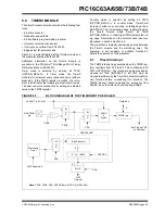
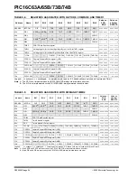
6.3
Prescaler
There is only one prescaler available which is mutually
exclusively shared between the Timer0 module and the
watchdog timer. A prescaler assignment for the Timer0
module means that there is no prescaler for the Watch-
dog Timer, and vice-versa. This prescaler is not read-
able or writable (see Figure 6-1).
The PSA and PS2:PS0 bits (OPTION_REG<3:0>)
determine the prescaler assignment and prescale ratio.
When assigned to the Timer0 module, all instructions
writing to the TMR0 register (e.g.,
CLRF
1,
MOVWF
1,
BSF
1,x
....etc.) will clear the prescaler. When assigned
to WDT, a
CLRWDT
instruction will clear the prescaler
along with the Watchdog Timer. The prescaler is not
readable or writable.
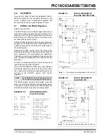
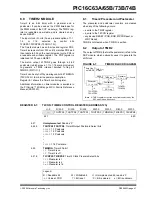
REGISTER 6-1:
OPTION_REG REGISTER
Note:
Writing to TMR0, when the prescaler is
assigned to Timer0, will clear the prescaler
count, but will not change the prescaler
assignment.
R/W-1
R/W-1
R/W-1
R/W-1
R/W-1
R/W-1
R/W-1
R/W-1
RBPU
INTEDG
T0CS
T0SE
PSA
PS2
PS1
PS0
bit 7
bit 0
bit 7
RBPU
bit 6
INTEDG
bit 5
T0CS: TMR0 Clock Source Select bit
1
= Transition on T0CKI pin
0
= Internal instruction cycle clock (CLKOUT)
bit 4
T0SE: TMR0 Source Edge Select bit
1
= Increment on high-to-low transition on T0CKI pin
0
= Increment on low-to-high transition on T0CKI pin
bit 3
PSA: Prescaler Assignment bit
1
= Prescaler is assigned to the WDT
0
= Prescaler is assigned to the Timer0 module
bit 2-0
PS2:PS0: Prescaler Rate Select bits
Legend:
R = Readable bit
W = Writable bit
U = Unimplemented bit, read as ‘0’
-n = Value at POR
’1’ = Bit is set
’0’ = Bit is cleared
x = Bit is unknown
000
001
010
011
100
101
110
111
1 : 2
1 : 4
1 : 8
1 : 16
1 : 32
1 : 64
1 : 128
1 : 256
1 : 1
1 : 2
1 : 4
1 : 8
1 : 16
1 : 32
1 : 64
1 : 128
Bit Value
TMR0 Rate
WDT Rate
Note:
To avoid an unintended device RESET, the instruction sequence shown in the PICmicro™ Mid-Range MCU
Family Reference Manual (DS33023, Section 11.6) must be executed when changing the prescaler assign-
ment from Timer0 to the WDT. This sequence must be followed even if the WDT is disabled.
Summary of Contents for PIC16C63A
Page 4: ...PIC16C63A 65B 73B 74B DS30605C page 4 2000 Microchip Technology Inc NOTES ...
Page 6: ...PIC16C63A 65B 73B 74B DS30605C page 6 2000 Microchip Technology Inc NOTES ...
Page 8: ...PIC16C63A 65B 73B 74B DS30605C page 8 2000 Microchip Technology Inc NOTES ...
Page 28: ...PIC16C63A 65B 73B 74B DS30605C page 28 2000 Microchip Technology Inc NOTES ...
Page 42: ...PIC16C63A 65B 73B 74B DS30605C page 42 2000 Microchip Technology Inc NOTES ...
Page 78: ...PIC16C63A 65B 73B 74B DS30605C page 78 2000 Microchip Technology Inc NOTES ...
Page 112: ...PIC16C63A 65B 73B 74B DS30605C page 112 2000 Microchip Technology Inc NOTES ...
Page 152: ...PIC16C63A 65B 73B 74B DS30605C page 152 2000 Microchip Technology Inc NOTES ...
Page 164: ...PIC16C63A 65B 73B 74B DS30605C page 164 2000 Microchip Technology Inc NOTES ...
Page 174: ...PIC16C63A 65B 73B 74B DS30605C page 174 2000 Microchip Technology Inc NOTES ...
Page 178: ...PIC16C63A 65B 73B 74B DS30605C page 178 2000 Microchip Technology Inc NOTES ...
Page 179: ... 2000 Microchip Technology Inc DS30605C page 179 PIC16C63A 65B 73B 74B NOTES ...
Page 180: ...PIC16C63A 65B 73B 74B DS30605C page 180 2000 Microchip Technology Inc NOTES ...
Page 181: ... 2000 Microchip Technology Inc DS30605C page 181 PIC16C63A 65B 73B 74B NOTES ...
Page 182: ...PIC16C63A 65B 73B 74B DS30605C page 182 2000 Microchip Technology Inc NOTES ...
Page 183: ... 2000 Microchip Technology Inc DS30605C page 183 PIC16C63A 65B 73B 74B NOTES ...


