61
LC89057W-VF4
No.7202-2/61
Continued from preceding page.
•
Outputs various information to make system configuration easy
−
Outputs DTS-CD/LD detection flag by DTS sync signal detection.
−
Outputs burst preamble Pc from microcontroller interface.
−
Calculates sampling frequency of input signal fs and outputs it from microcontroller interface.
−
Outputs interrupt signal for microcontroller (interrupt source can be selected).
−
Outputs signal of transitional period switching between VCO clock and oscillation amplifier clock.
−
Outputs bit 1 of channel status (non-PCM data detection bit).
−
Outputs emphasis information of channel status.
−
Outputs renewed flag of the first 48 bits channel status.
−
Validity flag and user data output are available.
−
Possible to carry out and output various settings through microcontroller interface.
•
Plenty of built-in functions to reduce peripheral circuits
−
Includes modulation function that can attach channel status, validity flag, and user data.
−
Equipped with a total of 7 digital data input pins: 1 input pin with an amplifier and 6 input pins with 5V tolerable
TTL level signal.
−
Possible to monitor input pin status with microcontroller by mounting a bi-phase input data detection function.
−
Possible to select input data among 8 system input data via PLL lock error.
−
Possible to select output of input-data-through among 8 system input data aside from selecting demodulation data.
−
Includes 2 system bit clock and LR clock outputs. Various dividing ratios can be set to one of these two systems.
−
Equipped with a serial digital audio data input pin. Possible to switch with demodulation output.
−
Possible to module the data that is input to the serial digital audio data input pin.
−
Includes built-in oscillation amplifier and frequency divider for quartz resonator and also possible to use them as
clock generator.
−
Includes 4 bits general-purpose parallel I/O port. It can be used for interface with peripheral LSI.
−
Single 3.3V-power supply operation. TTL input port supports 5V interface.
−
Adopts small SQFP48 package for efficient use of substrate mounting area.
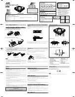
4. Pin Assignments
39
38
37
DI
RERR
SLRCK
SDIN
DO
36
42
41
40
45
44
43
48
47
46
CL
CE
DGND
XMODE
TMCK/PIO0
DVDD
TLRCK/PIO2
TBCK/PIO1
TXO/PIOEN
TDATA/PIO3
IN
T
35
C
K
S
T
34
A
U
D
IO
/V
O
33 32 31
LC89057W-VF4
Top view
DV
DD
30
XIN
29
E
M
P
H
A
/U
O
D
G
N
D
28 27
DV
DD
26
DV
DD
D
G
N
D
D
G
N
D
25
X
O
U
T
X
M
C
K
23
24
2
1
RDATA
SBCK
DVDD
RLRCK
RBCK
DGND
AGND
RMCK
LPF
AVDD
* R
X
5/
V
I
* R
X
6/
U
I
* : Pull-down resistor internal
DV
DD
* R
X
4
* R
X
3
D
G
N
D
R
X
1
* R
X
2
R
X
O
U
T
* R
X
0
4
3
6
5
8
7
10
9
12
11
21
22
19
20
17
18
15
16
13
14
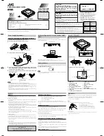
LC89057W-VF4
No.7202-4/61
6. Block Diagram
XMCK
XIN
XOUT
XMODE
CI
CE
CL
INT
AUDIO/VO
EMPHA/UO
RXOUT
CKST
Demodulation
&
Lock detect
Modulation
or
Parallel Port
Data
Selector
Clock
Selector
Microcontroller
I/F
1/N
PLL
Cbit, Ubit
Input
Selector
RX0
RX1
RX2
RX3
RX4
RX5/VI
TBCK/PIO1
TMCK/PIO0
RMCK
RBCK
SDIN
RDATA
RERR
DO
LPF
RX6/UI
TXO/PIOEN
TDATA/PIO3
TLRCK/PIO2
RLRCK
SBCK
SLRCK
1
10
9
8
5
4
3
2
13
44
45
46
47
48
33
32
35 48 39 38
41
21
37
36
22
23
20
17
16
24
29
28
27
34
Q501 : LC89057W-VF4