LTC4000
13
4000fb
For more information
operaTion
CSP pin (source). The controller (A1) regulates the external
PMOS by driving the gate of the PMOS device such that the
voltage drop across IID and CSP is 8mV (typical). When
the external PMOS ability to deliver a particular current
with an 8mV drop across its source and drain is exceeded,
the voltage at the gate clamps at V
IGATE(ON)
and the PMOS
behaves like a fixed value resistor (R
DS(ON)
).
Note that this input ideal diode function is only enabled
when the voltage at the IN pin is within its operating range
(3V to 60V). To ensure that the external PMOS is turned off
when the voltage at the IN pin is not within its operating
range, a 10M pull-up resistor between the IGATE and the
CSP pin is recommended.
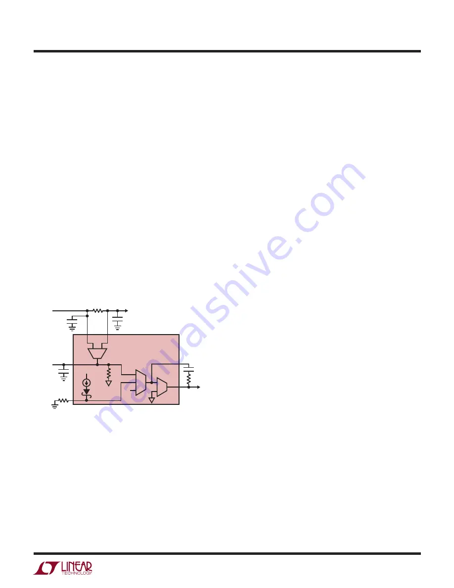
Input Current Regulation and Monitoring
One of the loops driving the ITH and CC pins is the input
current regulation loop (Figure 2). This loop prevents
the input current sensed through the input current sense
resistor (R
IS
) from exceeding the programmed input
current limit.
or open, the bad battery detection timer is enabled. When
this bad battery detection timer expires and the battery volt-
age is still below V
LOBAT
, the battery charger automatically
terminates and indicates, via the
FLT
and
CHRG
pins, that
the battery was unresponsive to charge current.
Once the battery voltage is above V
LOBAT
, the charge current
regulation loop begins charging in full power constant-
current mode. In this case, the programmed full charge
current is set with a resistor on the CL pin.
Depending on available input power and external load
conditions, the battery charger may not be able to charge
at the full programmed rate. The external load is always
prioritized over the battery charge current. The input
current limit programming is always observed, and only
additional power is available to charge the battery. When
system loads are light, battery charge current is maximized.
Once the float voltage is achieved, the battery float volt-
age regulation loop takes over from the charge current
regulation loop and initiates constant voltage charging. In
constant voltage charging, charge current slowly declines.
Charge termination can be configured with the TMR pin
in several ways. If the TMR pin is tied to the BIAS pin,
C/X termination is selected. In this case, charging is
terminated when constant voltage charging reduces the
charge current to the C/X level programmed at the CX
pin. Connecting a capacitor to the TMR pin selects the
charge timer termination and a charge termination timer
is started at the beginning of constant voltage charging.
Charging terminates when the termination timer expires.
When continuous charging at the float voltage is desired,
tie the TMR pin to GND to disable termination.
Upon charge termination, the PMOS connected to BGATE
behaves as an ideal diode from BAT to CSN. The diode
function prevents charge current but provides current
to the system load as needed. If the system load can be
completely supplied from the input, the battery PMOS turns
off. While terminated, if the input current limit is not in
regulation, the output voltage regulation loop takes over to
ensure that the output voltage at CSP remains in control.
The output voltage regulation loop regulates the voltage
at the CSP pin such that the output feedback voltage at
the OFB pin is 1.193V.
Figure 2. Input Current Regulation Loop
Battery Charger Overview
In addition to the input current regulation loop, the
LTC4000 regulates charge current, battery voltage and
output voltage.
When a battery charge cycle begins, the battery charger
first determines if the battery is over-discharged. If the bat-
tery feedback voltage is below V
LOBAT
, an automatic trickle
charge feature uses the charge current regulation loop to
set the battery charge current to 10% of the programmed
full scale value. If the TMR pin is connected to a capacitor
IN
CC
1V
A8
A8
g
m
= 0.33m
ITH
LTC4000
IN
CLN
R
IS
LOAD
C
CLN
(OPTIONAL)
IIMON
IL
C
IIMON
(OPTIONAL)
C
IN
+
–
–
+
+
–
–
C
C
TO DC/DC
4000 FO2
R
C
60k
50µA
BIAS
R
IL
A4


