


13
LTC1624
100
Ω
resistor in series with the SENSE
–
pin. This offset
cancels the internal offset in current comparator I
2
(refer
to Functional Diagram). This comparator in conjunction
with the voltage on the I
TH
/RUN pin determines when to
enter into Burst Mode operation (refer to Low Current
Operation in Operation section). With the additional exter-
nal offset present, the drive to the topside MOSFET is
always enabled every cycle and constant frequency opera-
tion occurs for I
OUT
> I
OUT(MIN)
.
Step-Down Converter: Design Example
As a design example, assume V
IN
= 12V(nominal),
V
IN
= 22V(max), V
OUT
= 3.3V and I
MAX
= 2A. R
SENSE
can
immediately be calculated:
R
SENSE
= 100mV/2A = 0.05
Ω
Assume a 10
µ
H inductor. To check the actual value of the
ripple current the following equation is used:
∆
I
V
V
f L
V
V
V
V
L
IN
OUT
OUT
D
IN
D
=
−
( )( )
+
+
The highest value of the ripple current occurs at the
maximum input voltage:
∆
I
V
V
kHz
H
V
V
V
V
L
=
−
( )
+
+
=
22
3 3
200
10
3 3
0 5
22
0 5
1 58
.
.
.
.
.
µ
A
P-P
The power dissipation on the topside MOSFET can be
easily estimated. Choosing a Siliconix Si4412DY results
in: R
DS(ON)
= 0.042
Ω
, C
RSS
= 100pF. At maximum input
voltage with T(estimated) = 50
°
C:
P
V
V
V
V
A
C
C
V
A
pF
kHz
mW
MAIN
=
+
+
( )
+
( )
° − °
(
)
[
]
(
)
+
( ) ( )( )(
)
=
3 3
0 5
22
0 5
2
1
0 005 50
25
0 042
2 5 22
2
100
200
62
2
1 85
.
.
.
.
.
.
.
Ω
The most stringent requirement for the Schottky diode
occurs when V
OUT
= 0V (i.e. short circuit) at maximum V
IN
.
In this case the worst-case dissipation rises to:
P
I
V
V
V
V
D
SC AVG
D
IN
IN
D
=
( )
+
( )
APPLICATIO
N
S I
N
FOR
M
ATIO
N
W
U
U
U
With the 0.05
Ω
sense resistor I
SC(AVG)
= 2A will result,
increasing the 0.5V Schottky diode dissipation to 0.98W.
C
IN
is chosen for an RMS current rating of at least 1.0A at
temperature. C
OUT
is chosen with an ESR of 0.03
Ω
for low
output ripple. The output ripple in continuous mode will be
highest at the maximum input voltage. The output voltage
ripple due to ESR is approximately:
V
ORIPPLE
= R
ESR
(
∆
I
L
) = 0.03
Ω
(1.58A
P-P
) = 47mV
P-P
Step-Down Converter: Duty Cycle Limitations
At high input to output differential voltages the on-time
gets very small. Due to internal gate delays and response
times of the internal circuitry the minimum recommended
on-time is 450ns. Since the LTC1624’s frequency is inter-
nally set to 200kHz a potential duty cycle limitation exists.
When the duty cycle is less than 9%, cycle skipping may
occur which increases the inductor ripple current but does
not cause V
OUT
to lose regulation. Avoiding cycle skipping
imposes a limit on the input voltage for a given output
voltage only when V
OUT
< 2.2V using 30V MOSFETs.
(Remember not to exceed the absolute maximum voltage
of 36V.)
V
IN(MAX)
= 11.1V
OUT
+ 5V For DC > 9%
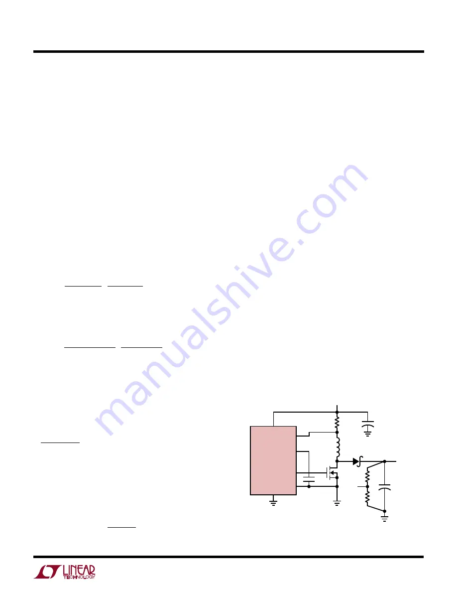
Boost Converter Applications
The LTC1624 is also well-suited to boost converter appli-
cations. A boost converter steps up the input voltage to a
higher voltage as shown in Figure 6.
Figure 6. Boost Converter
+
C
B
L1
M1
R2
R1
R
SENSE
C
IN
D1
V
IN
1624 F06
V
IN
V
FB
LTC1624
SENSE
–
BOOST
TG
SW
GND
+
C
OUT
V
OUT


