


LT8611
19
8611fa
For more information
APPLICATIONS INFORMATION
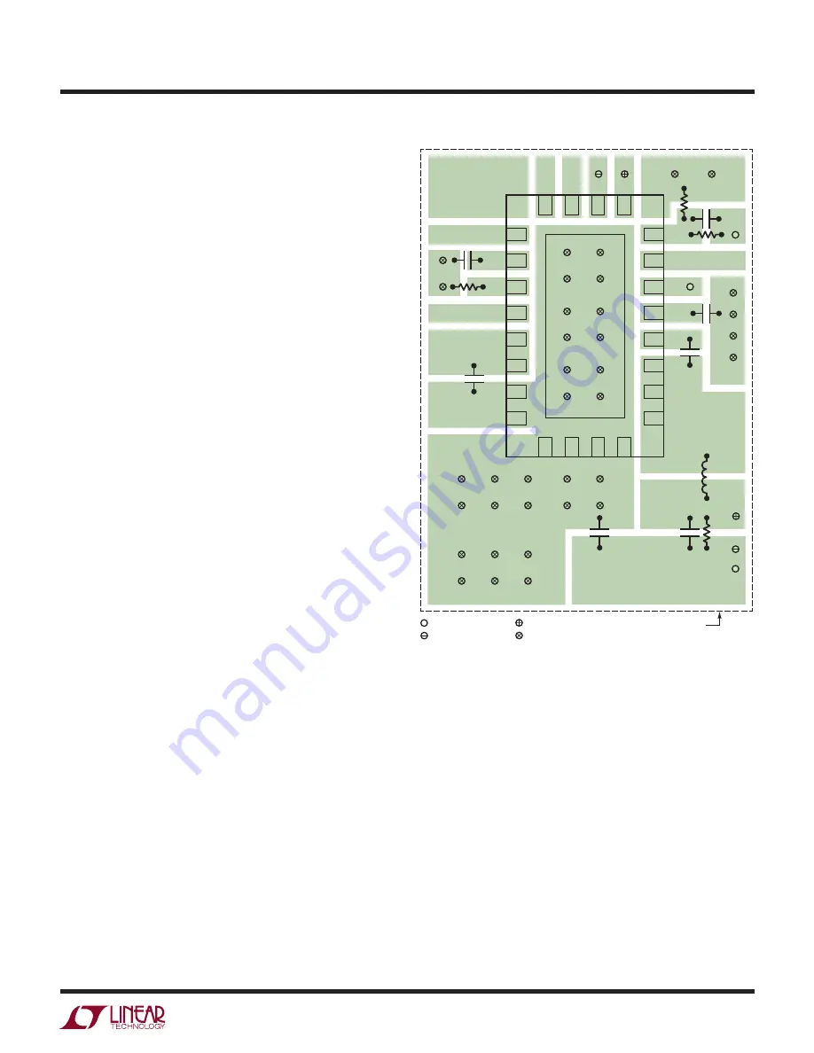
Figure 6. Recommended PCB Layout for the LT8611
PCB Layout
For proper operation and minimum EMI, care must be taken
during printed circuit board layout. Figure 6 shows the
recommended component placement with trace, ground
plane and via locations. Note that large, switched currents
flow in the LT8611’s V
IN
pins, PGND pins, and the input ca-
pacitor (C1). The loop formed by the input capacitor should
be as small as possible by placing the capacitor adjacent
to the V
IN
and PGND pins. When using a physically large
input capacitor the resulting loop may become too large
in which case using a small case/value capacitor placed
close to the V
IN
and PGND pins plus a larger capacitor
further away is preferred. These components, along with
the inductor and output capacitor, should be placed on
the same side of the circuit board, and their connections
should be made on that layer. Place a local, unbroken ground
plane under the application circuit on the layer closest to
the surface layer. The SW and BOOST nodes should be
as small as possible. Finally, keep the FB and RT nodes
small so that the ground traces will shield them from the
SW and BOOST nodes. The exposed pad on the bottom of
the package must be soldered to ground so that the pad
is connected to ground electrically and also acts as a heat
sink thermally. To keep thermal resistance low, extend the
ground plane as much as possible, and add thermal vias
under and near the LT8611 to additional ground planes
within the circuit board and on the bottom side.
High Temperature Considerations
For higher ambient temperatures, care should be taken in
the layout of the PCB to ensure good heat sinking of the
LT8611. The exposed pad on the bottom of the package
must be soldered to a ground plane. This ground should be
tied to large copper layers below with thermal vias; these
layers will spread heat dissipated by the LT8611. Placing
additional vias can reduce thermal resistance further. The
maximum load current should be derated as the ambient
temperature approaches the maximum junction rating.
Power dissipation within the LT8611 can be estimated
by calculating the total power loss from an efficiency
measurement and subtracting the inductor loss. The
die temperature is calculated by multiplying the LT8611
power dissipation by the thermal resistance from junction
to ambient. The LT8611 will stop switching and indicate
a fault condition if safe junction temperature is exceeded.
9
10
11
12
V
OUT
8611 F06
OUTLINE OF LOCAL
GROUND PLANE
GND
13
14
15
16
17
18
19
PG
FB
BIAS
BST
SW
INTV
CC
V
OUT
20
21
22
23
IMON
ISN
ISP
GND
ICTRL
SYNC
TR/SS
RT
EN/UV
V
IN
24
1
2
3
4
5
6
7
8
V
OUT
LINE TO BIAS
V
OUT
LINE TO ISN
LINE TO ISP
VIAS TO GROUND PLANE


