4
dc2194af
DEMO MANUAL DC2194A
Quick start proceDure
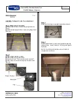
Demonstration circuit DC2194A is easy to set up to evaluate
the performance of the LTM4642. Please refer to Figure 1
for proper measurement equipment setup and follow the
procedures below:
1. With power off, connect the input power supply at V
IN
(J4) and GND (J5)
2. Connect the first load between V
OUT1
(J6) and GND
(J7) for Channel 1, connect the second load between
V
OUT2
(J8) and GND (J3) for Channel 2. Preset all the
loads to 0A.
3. Connect the DMMs at the input (E4 and E5) to moni-
tor input voltage. Connect DMMs at V
O1
+ (E6) and
V
O1
– (E7), V
O2
+ (E11) and V
O2
– (E9) to monitor DC
output voltages. These output voltage test points are
Kelvin sensed directly across C
OUT1
for Channel 1 and
C
OUT4
for Channel 2 to provide accurate measurement
of output voltages. Do not apply load current to any of
the above test points to avoid damage to the regulator.
Do not connect the ground leads of scope probes to
V
O1
– and V
O2
–.
4. Turn on the power supply at the input. Measure and
make sure the input supply voltage is 12V. Place the
RUN 1 (JP4) and RUN2 (JP5) in the “ON” position. The
output voltage should be 1.8V ±1.5% for Channel 1 and
1.2 ±1.5% for Channel 2.
5. Once the input and output voltages are properly estab-
lished, adjust the input voltage between 4.5V and 20V
and the loads within the operating range of 0A to 4A
max per channel. Observe the output voltage regula-
tion, output voltage ripples, switch node waveform,
load transient response and other parameters. Refer to
Figure 2 for proper output voltage ripple measurement.
NOTE 1: To measure the input/output voltage ripple
properly, do not use the long ground lead on the
oscil loscope probe. See Figure 2 for the proper scope
probe placement technique. Short, still leads need to
be soldered to the (+) and (–) terminals of an output
capacitor. The probe’s ground ring needs to touch the
(–) lead and the probe tip needs to touch the (+) lead.
6. DC2194A provides convenient on board BNC terminals
to accurately measure output ripples of Channel 1 and
Channel 2. Connect short BNC cables from V
OUT1
,
V
OUT2
to the scope inputs (Scope probe ratio 1:1, AC
coupling) to observe output voltage ripples.
7. DC2194A provides an optional onboard load transient
circuit to measure ∆V
OUT
peak-to-peak deviation dur-
ing rising or falling dynamic load transient. The simple
load step circuit consisting of a 30V N-channel power
MOSFET in series with a 10mΩ, 1W,1% current sense
resistor. The MOSFET is configured as a voltage control
current source (VCCS) device, therefore the output cur-
rent step and its magnitude is created and controlled by
adjusting the amplitude of the applied input voltage step
at the gate of the MOSFET. Use a function generator to
provide a voltage pulse between IOSTEP CLK (E17) and
GND (E18); the input voltage pulse should be set at the
frequency less than 10Hz and maximum duty cycle of
less than 5% to avoid excessive thermal stress on the
MOSFET device. The output current step is measured
directly across the 10mΩ current sense resistor and
monitored by connecting a BNC cable from IOSTEP to
the input of the oscilloscope (scope probe ratio 1:1,
DC coupling), the equivalent voltage to current scale
is 10mV/1A. The load step current slew rate dI/dt can
be set by adjusting the rising time and fall time of the
input voltage pulse.
The default load step circuit is connected to V
OUT1
but
can be used for V
OUT2
by simply removing the zero
Ohm jumper R27 and stuffing it at the position of R28
and vice versa. Repeat Step 7 to perform load step
transient evaluation for Channel 2.